
Adjustment method of bimetal gate work function

An adjustment method and double metal gate technology, applied in the manufacture of electrical components, circuits, semiconductors/solid-state devices, etc., to achieve good thermal stability and adjust the work function of metal gates, facilitate industrialization, and the method is simple and easy to implement

Active Publication Date: 2010-08-11
INST OF MICROELECTRONICS CHINESE ACAD OF SCI
View PDF2 Cites 26 Cited by
  • Summary
  • Abstract
  • Description
  • Claims
  • Application Information

AI Technical Summary

Problems solved by technology

However, there are still many problems to be solved when metal gates are integrated on high-K gate dielectrics, such as thermal stability problems, interface state problems, especially the Fermi pinning effect, which makes it difficult to obtain the appropriate low threshold voltage required by nano-CMOS devices. big challenge

Method used


Image

  • Adjustment method of bimetal gate work function
  • Adjustment method of bimetal gate work function

Examples


Embodiment Construction

[0018] Step 1. Cleaning: After the device isolation is formed, perform the cleaning before the formation of the interface oxide layer. First, use conventional methods to clean, and then use hydrofluoric acid: isopropanol: water (weight ratio) = 0.3-0.8%: 0.01-0.08 %:1% mixed solution soak for 2-10 minutes at room temperature, rinse with deionized water, N 2 Enter the furnace immediately after spinning dry;

[0019] Step 2. Formation of interface layer SiOx: at 600-800℃, in N 2 Moderate rapid thermal annealing (RTA) 20-120 seconds; 5-8 的oxide layer;

[0020] Step 3. Formation of high dielectric constant (K) gate dielectric film: using PVD method, using magnetron reactive sputtering process in N 2 / Ar atmosphere alternately sputtering Hf-La target and Hf target deposition to form HfLaON, the working pressure of sputtering is 5×10 -3 Torr, the sputtering power is 100-500W, and the thickness of the deposited HfLaON high-k gate dielectric film is 10-60 angstroms;

[0021] Step 4. Ultraso...


PUM

PropertyMeasurementUnit
thicknessaaaaaaaaaa

Abstract

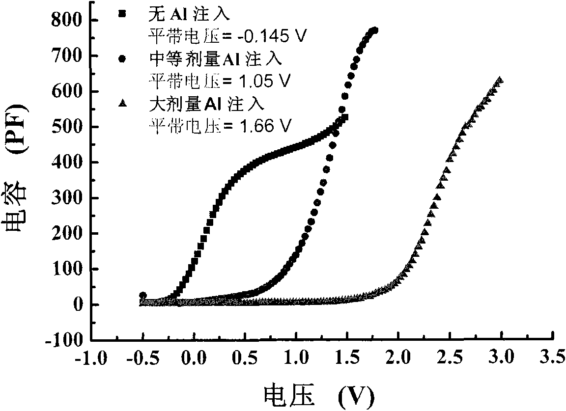
The invention relates to an adjustment method of a bimetal gate work function, which mainly comprises the following steps: (1) growing a ultrathin interface oxide layer or a nitrogen oxide layer through rapid thermal oxidation; (2) alternately sputtering and depositing gate dielectrics with a high dielectric constant (K) on the ultrathin interface oxide layer through reactive magnetron sputtering; (3) after the gate dielectrics with the high K are deposited, carrying out rapid thermal annealing; (4) depositing metal nitride gates through reactive magnetron sputtering; (5) injecting metal ions for doping the metal nitride gates; and (6) after metal gate electrodes are formed by etching, carrying out rapid thermal annealing to drive the metal ions onto the interfaces of the metal gates and the gate dielectrics with the high K. The method can be simply and easily realized, has good thermal stability and capacity of adjusting a metal gate work function, is completely compatible with the CMOS process, and is convenient for industrialization of integrated circuits.

Description

Technical field [0001] The invention belongs to the field of semiconductor technology, and particularly refers to a method for adjusting the work function of a double metal gate, which is suitable for the application of a high-performance nano-complementary metal oxide semiconductor (CMOS) device of 32 nanometers and below. Background technique [0002] As the feature size of CMOS devices continues to shrink, the application of high dielectric constant (K) gate dielectrics and metal gate electrodes is imperative. Using a high-K dielectric, due to its relatively thick physical thickness under the same equivalent oxide thickness (EOT), the gate tunneling leakage current can be greatly reduced. However, the traditional polysilicon gate is not compatible with the high-K gate dielectric, and there is a serious Fermi pinning effect, so a new type of metal gate electrode must be used instead. The metal gate can not only eliminate the depletion effect of the polysilicon gate and reduce ...

Claims


Application Information

Patent Timeline
Patent Type & Authority Applications(China)
IPC IPC(8): H01L21/8238H01L21/283H01L21/265
Inventor 徐秋霞许高博
Owner INST OF MICROELECTRONICS CHINESE ACAD OF SCI
Learn More