Ultra-fine cone electrode array and method for manufacturing same

A technology of electrode arrays and ultra-micro electrodes, which is applied in the field of micro-sensing, can solve the problems of affecting the range of use of ultra-micro electrode arrays, lack of wide-scale promotion and application, and high cost, so as to reduce the difficulty of preparation, increase the aspect ratio, and reduce the cost. cheap effect

Inactive Publication Date: 2010-08-18
XI AN JIAOTONG UNIV
View PDF0 Cites 5 Cited by
  • Summary
  • Abstract
  • Description
  • Claims
  • Application Information

AI Technical Summary

Problems solved by technology

For the preparation of ultra-micro-electrode arrays by micro-fabrication technology, there are two limitations: to obtain nano-scale feature size, it is necessary to further improve plate-making technology, pattern transfer technology, etching technology, etc., and these technologies have strict requirements on equipment and environment, and cost Expensive; on the other hand, it is not easy to obtain a three-dimensional electrode structure with a feature size of less than 100nm and a large aspect ratio with this technology
Although the combination of soft lithography and

Method used


Image

  • Ultra-fine cone electrode array and method for manufacturing same
  • Ultra-fine cone electrode array and method for manufacturing same
  • Ultra-fine cone electrode array and method for manufacturing same

Examples


Embodiment Construction

[0039] The present invention will be further described in detail below in conjunction with the accompanying drawings and embodiments.

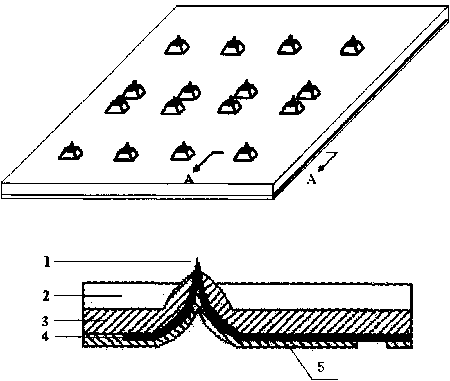
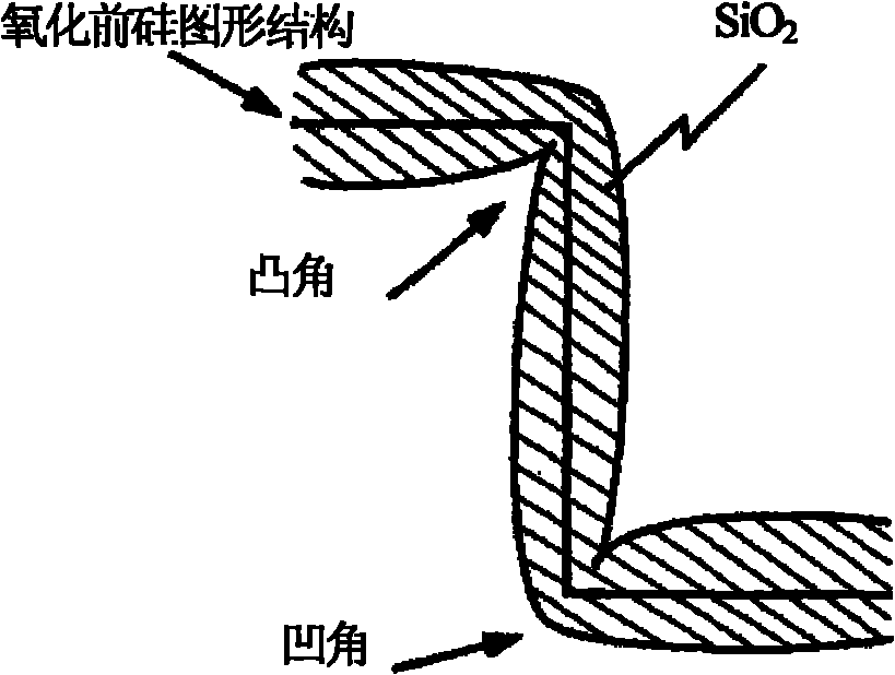
[0040] see figure 1 , the ultra-micro-cone electrode array of the present invention includes a single-sided polished silicon wafer 2 as a substrate, and the single-sided polished silicon wafer adopts p-Si (100) with a resistivity of 0.01-0.1Ω·cm, and the thickness of the substrate is 200 μm , and several groups of regular pyramidal pits with a taper angle of 70.52° in the silicon wafer 2, and a layer of SiO with inconsistent thickness covering the silicon wafer 2 and the regular quadrangular pyramidal pits 2 Thin film 3, on SiO 2 A layer of 400nm and patterned conductive metal film electrode material layer 4 is provided on the surface of the film 3, and a 700nm and patterned Si layer is provided on the conductive metal film electrode material layer 4. 3 N 4 protective film5.

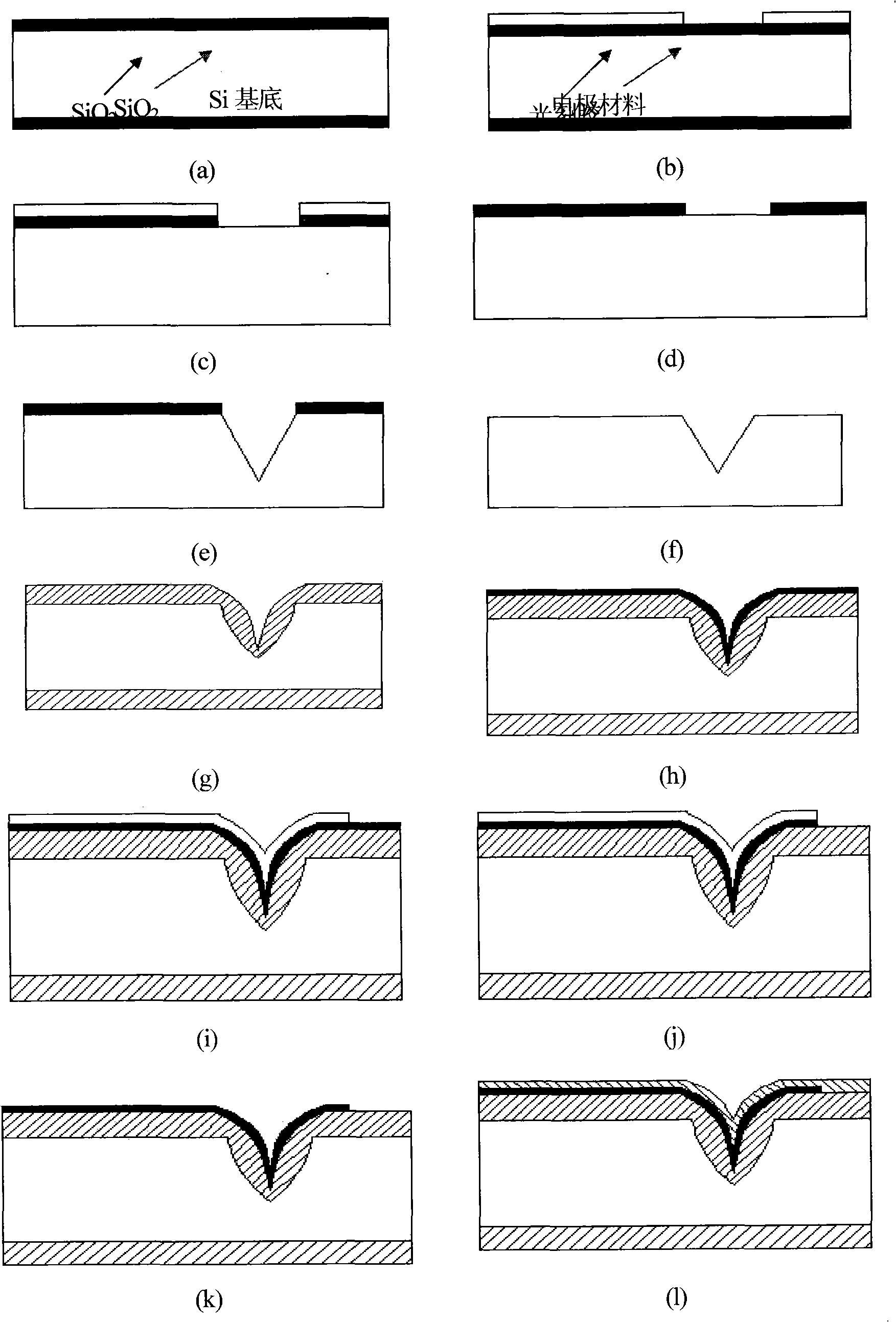
[0041] The manufacture process of the present invention sees ...


PUM

PropertyMeasurementUnit
Resistivityaaaaaaaaaa
Thicknessaaaaaaaaaa
Cone angleaaaaaaaaaa

Abstract

The invention relates to an ultra-fine cone electrode array and a method for manufacturing the same. The method for manufacturing the nano-size ultra-fine cone electrode array comprises the following steps: oxidizing a silicon slice with the wet process and the dry process to form an SiO2 film on the silicon slice, and photoetching a rectangular window on the SiO2 film by using positive photoresist; etching the silicon slice exposed in the rectangular window on the SiO2 film with the wet process by using the TMAH solution to form a pit in the rectangular pyramid shape, and removing the left SiO2 film; thermally oxidizing the silicon slice at 950 DEG C to form an SiO2 film, sputtering ultra-fine electrode material on the surface of the silicon slice, which is provided with the pit, with the radio-frequency magnetron sputtering process, and forming a ultra-fine electrode position and a lead wire pattern with the photoetching process and the etching process; depositing an Si3N4 film on the surface of the ultra-fine electrode material with the vapor-phase deposition process, and photoetching and etching a window on the Si3N4 film with the photoetching process and the etching process so as to expose an ultra-fine electrode bonding window; thinning and etching the back surface of the silicon slice by using the TMAH solution until an SiO2 lug boss being exposed, and etching the SiO2 lug boss until ultra-fine electrodes with a certain height ratio being exposed.

Description

technical field [0001] The invention belongs to the field of micro-sensing technology, and is mainly used in biology, medicine, electrochemistry and environmental monitoring, etc., and particularly relates to an ultra-micro-cone electrode array for information recording and electrical stimulation of micro-regions such as cells and nerves and its preparation method. Background technique [0002] The ultra-micro-cone electrode array and its preparation method belong to the field of micro-sensing technology, and are mainly used in biology, medicine, electrochemistry, environmental monitoring and the like. In the fields of biology and medicine, ultra-micro electrode arrays are mainly used to record information such as brain and retina slices, cardiomyocytes, ion channel screening, pharmacology, plastic deformation of nerve axons, circadian rhythms, nerve regeneration, and micro-EEG. and electrical stimulation. In terms of electrochemical applications, ultramicroelectrode array...

Claims


Application Information

Patent Timeline
IPC IPC(8): B81B7/02B81C1/00
Inventor 景蔚萱蒋庄德朱明智周贵庭杜明贤王琛英赵凤霞
Owner XI AN JIAOTONG UNIV
Why Eureka
Try Eureka