Three-sided silicified gate metallic oxide semiconductor field effect transistor and preparation method thereof

An oxide semiconductor and field effect transistor technology, applied in the field of semiconductor devices and their fabrication processes, can solve the problems of increasing gate resistance, limiting the improvement and upgrading of LDMOSFET device performance, and reducing the gate resistance of the device and optimizing the device. performance, the effect of good device performance

Inactive Publication Date: 2012-05-16
TSINGHUA UNIV
View PDF0 Cites 0 Cited by
  • Summary
  • Abstract
  • Description
  • Claims
  • Application Information

AI Technical Summary

Problems solved by technology

However, the above-mentioned LDMOSFET metal silicide technical solution obviously has obvious disadvantages, that is, the protective dielectric layer 232 covering the lightly doped drain drift region 222 needs to be formed by photolithography, so considering the registration deviation of the photolithography mask The problem is that the protective dielectric layer 232 must ensure a certain coverage on the polysilicon gate 218, so this technology is essentially a non-salicide technology, which makes it possible for the polysilicon gate 218 to form low-resistance metal silicide only on part of the surface objects, that is, partially silicided gate schemes, such as figure 2 shown, the polysilicon gate silicide length L S = polysilicon gate length L G - Cover length L O , that is, the length of the polysilicon gate silicide is smaller than the length of the polysilicon gate, which leads to an increase in the corresponding gate resistance (because the gate current direction basically flows along the gate width direction perpendicular to the gate length, the cross section of the gate current and the gate length is directly proportional to the gate resistance, so the gate resistance is basically inversely proportional to the gate length), especially considering the technical route of continuously shrinking the feature size of the device in order to continuously improve the performance of the device under the current semiconductor technology background, this will make polysilicon The problem of increased gate resistance caused by shortened gate length is becoming more and more prominent, which seriously limits the improvement and upgrade of LDMOSFET device performance

Method used


Image

  • Three-sided silicified gate metallic oxide semiconductor field effect transistor and preparation method thereof
  • Three-sided silicified gate metallic oxide semiconductor field effect transistor and preparation method thereof
  • Three-sided silicified gate metallic oxide semiconductor field effect transistor and preparation method thereof

Examples


Embodiment Construction

[0034] Firstly, taking the preparation of a MOSFET with low gate resistance as an example, the specific implementation of the three-side silicided gate metal silicide solution proposed by the present invention and the device fabrication process flow are introduced.

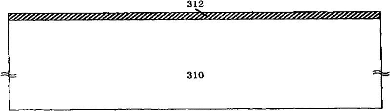
[0035] 1. As shown in FIG. 3.1 , a gate dielectric (some dielectric) layer 312 is thermally grown or deposited on a silicon substrate 310 of the first conductivity type. Before or after forming the gate dielectric layer 312 , ion implantation is performed into the substrate 310 to achieve the purpose of adjusting the threshold voltage of the finally fabricated device.

[0036] 2. As shown in Figure 3.2, deposit a polysilicon layer 314 on the gate dielectric layer 312, and make it a heavily doped polysilicon layer by in-situ doping during deposition or ion implantation after deposition.

[0037] 3. As shown in Figure 3.3, heavy doping is formed by photolithography and etching (the doping concentration is 1×10 19 / ...


PUM


Abstract

The invention discloses a three-sided silicified gate metallic oxide semiconductor field effect transistor and a preparation method thereof, belonging to the technical field of manufacturing a semiconductor apparatus. The invention comprises preparations of a low-gate resistance metallic oxide semiconductor field effect transistor and a transverse double-diffused metallic oxide semiconductor field effect transistor with three-sided silicon gate metallic silicide structures. In the method, by adopting the masking effect of a gate dielectric layer reserved after being etched by a polysilicon gate, the three-sided silicified gate metallic silicide structures are formed on the upper surface of the polysilicon gate and the source terminal side and the drain terminal side opposite to the polysilicon gate, a source-region metallic silicide is formed on the surface of a heavily doped source region, and a drain-region metallic silicide is formed on the surface of a heavily doped drain region. In the invention, the silicide can be formed on the surfaces of the gate, thus increasing the effective section of grid current, providing basis for continuously reducing characteristic dimensions of the apparatus, and obtaining lower gate resistance and better apparatus performances on the premise of non-sacrificial breakdown voltage of the apparatus.

Description

technical field [0001] The invention relates to the technical field of semiconductor devices and their preparation technology, in particular to a three-side silicided gate metal oxide semiconductor field effect transistor with low gate resistance and a preparation method thereof, in particular to a lateral double-diffused metal oxide with low gate resistance Fabrication process of semiconductor field effect transistors. Background technique [0002] The gate of a Metal Oxide Semiconductor Field Effect Transistor (hereinafter referred to as MOSFET) introduces a gate series resistance. Although the MOSFET is an insulated gate field effect transistor, the gate has no quiescent current, so the gate resistance has no effect on its DC working state, but if the device works in the AC state, especially for high-speed, radio frequency and microwave MOSFETs, the gate Resistance will play a decisive role in determining key performance indicators such as operating speed and power gain ...

Claims


Application Information

Patent Timeline
Patent Type & Authority Patents(China)
IPC IPC(8): H01L29/78H01L29/40H01L21/336H01L21/28
Inventor 付军王玉东吴正立许平崔杰蒋志朱从益赵悦
Owner TSINGHUA UNIV
Why Eureka
Try Eureka