Gate stack structure for semiconductor flash memory device and preparation method thereof

A flash memory device and gate stack technology, applied in the fields of semiconductor/solid-state device manufacturing, semiconductor devices, electric solid-state devices, etc., can solve the problems of slow operation speed and high operating voltage, increase electric field strength, improve storage density, and reduce operation. The effect of voltage

Inactive Publication Date: 2010-11-17
FUDAN UNIV
View PDF0 Cites 10 Cited by
  • Summary
  • Abstract
  • Description
  • Claims
  • Application Information

AI Technical Summary

Problems solved by technology

However, the disadvantage of this structure memory is that its operating voltage is high and the operating speed is slow [5]

Method used


Image

  • Gate stack structure for semiconductor flash memory device and preparation method thereof
  • Gate stack structure for semiconductor flash memory device and preparation method thereof
  • Gate stack structure for semiconductor flash memory device and preparation method thereof

Examples


Embodiment Construction

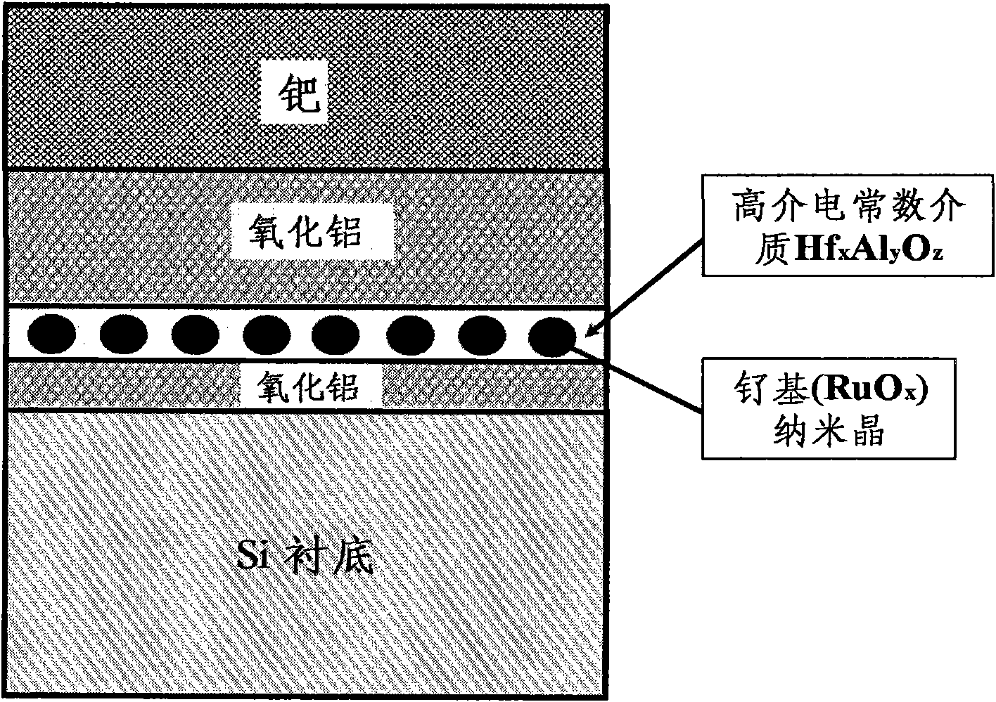
[0038] The preparation method of the novel gate stack structure flash storage capacitor proposed by the present invention is as follows:

[0039] (1) A P-type single crystal silicon wafer with (100) crystal orientation is used as the substrate, and the resistivity of the silicon wafer is 8-12 ohm·cm. Silicon wafers are first cleaned as standard, and the residual native oxide layer is removed with dilute hydrofluoric acid.

[0040] (2) Tunneling layer Al 2 o 3 The formation of: using trimethylaluminum and water vapor as the reaction source, the method of atomic layer deposition is used to grow Al 2 o 3 For thin films, the substrate temperature is controlled within the range of 250-350°C. Al 2 o 3 The thickness of the tunneling layer is controlled within the range of 5-10 nanometers.

[0041] (3) Nanocrystalline RuO in the heterogeneous charge-trapping layer x The formation: using magnetron sputtering deposition method, in Al 2 o 3 Deposit an ultra-thin metal ruthenium...


PUM

PropertyMeasurementUnit
thicknessaaaaaaaaaa
thicknessaaaaaaaaaa
thicknessaaaaaaaaaa

Abstract

The invention belongs to the technical field of manufacturing technology of semiconductor integrated circuits, and in particular relates to a gate stack structure for a flash memory device and a preparation method thereof. The gate stack structure comprises an Al2O3 thin film, ruthenium-based nanocrystals, a HfxAlyOz thin film, an Al2O3 thin film and a top electrode layer from bottom to top in turn by taking a silicon slice in P-type (100) crystal orientation as a substrate, wherein the Al2O3 thin film is used as a charge tunneling layer; the ruthenium-based nanocrystals are used as a first charge trapping layer; the HfxAlyOz thin film is used as a second charge trapping layer; and the Al2O3 thin film is used as a charge barrier layer. In the invention, the ruthenium-based nanocrystals have high thermal stability and are difficult to diffuse at a high temperature; the HfxAlyOz thin film has high charge trapping density; and the top electrode is made of metal palladium and has large work function. Thus the gate stack structure has broad application prospect in nanocrystalline memory capacitors.

Description

technical field [0001] The invention belongs to the technical field of semiconductor integrated circuit manufacturing, and in particular relates to a capacitor structure and a preparation method of a flash memory, in particular to a novel heterogeneous charge trapping layer based on metal nanocrystals and high dielectric constant media and a preparation method. Background technique [0002] With the continuous development of semiconductor process technology, the integration density of non-volatile flash memory is getting higher and higher, and the operating voltage is getting lower and lower, which drives the continuous reduction of device feature size. After the 65nm technology node, the traditional polysilicon floating gate structure There are a series of problems that greatly affect the performance of device storage, such as slow erasing and writing speed, high operating voltage, etc. [1]. A new generation of non-volatile memory based on discontinuous charge trapping mech...

Claims


Application Information

Patent Timeline
Patent Type & Authority Applications(China)
IPC IPC(8): H01L29/49H01L21/285H01L27/115
CPCC23C16/40B82Y10/00H01L21/28273H01L29/42332C23C16/45525H01L21/28079H01L29/4234C23C16/00H01L21/28282H01L29/495H01L29/40114H01L29/40117
Inventor 丁士进苟鸿雁张卫
Owner FUDAN UNIV
Why Eureka
Try Eureka