Method for manufacturing three-dimensional smooth curved surface microstructure based on SU-8 thick photo-resist
A production method, SU-8 technology, applied in the direction of microstructure technology, microstructure device, manufacturing microstructure device, etc., can solve the problems of high glass transition temperature, difficult to use positive photoresist reflow method, etc. simple effect
- Summary
- Abstract
- Description
- Claims
- Application Information
AI Technical Summary
Problems solved by technology
Method used
Image
Examples
Embodiment 1
[0016] The substantive features and remarkable progress of the present invention will be further described below in conjunction with the accompanying drawings using SU-8 photoresist.
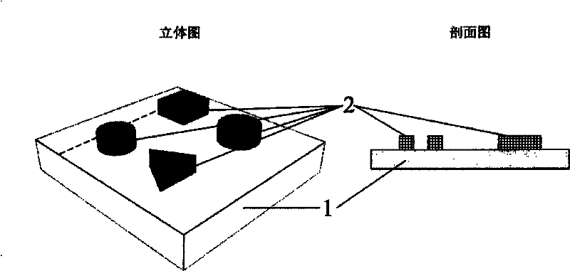
[0017] 1. Utilize SU-8 photoresist conventional process to make SU-8 original model, such as figure 1 shown.
[0018] 2. Mix the PDMS prepolymer and curing agent in a ratio of 10:1 (mass ratio), and vacuum degas (eliminate the bubbles formed by stirring and mixing the PDMS prepolymer and curing agent), and pour it into the SU- 8 on the original mold, and then placed on a hot plate at 85°C for 1 hour to cure.
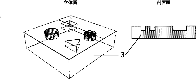
[0019] 3. Peel off the cured PDMS from the SU-8 master mold to make a PDMS master mold, such as figure 2 shown.
[0020] 4. Take the cleaned silicon wafer, bake at 150°C for 20 minutes, cool to room temperature, spin-coat SU-8 photoresist, place on a hot plate at 90°C and bake for 1 hour, then cool to room temperature.
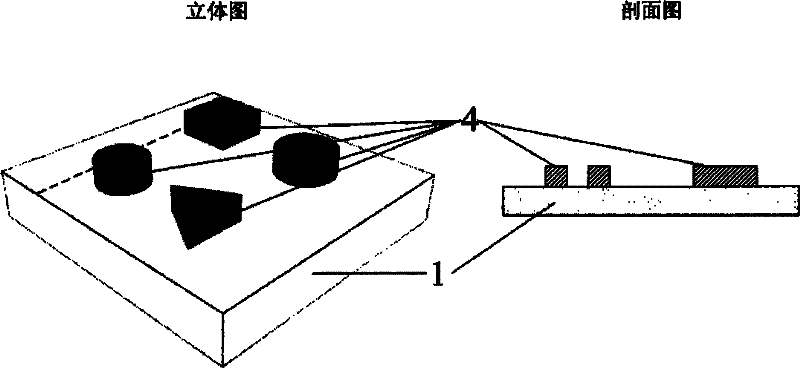
[0021] 5. After vacuum degassing the PDMS master mold prepared a...
Embodiment 2
[0024] Utilize the process method of making the SU-8 smooth surface microstructure that embodiment 1 proposes to make microlens arrays with different curvatures (such as Figure 5 shown), the curvature of the microlens can be controlled by adjusting the thickness of the SU-8 master mold and the size and shape design of the light-transmitting structure of the photolithography mask. The thickness of the SU-8 master mold is between 10 μm and 1000 μm, and the photolithography mask The shape of the light-transmitting structure of the stencil can be a regular polygon or a circle, and the side length or diameter is 10 μm-1000 μm. The fabricated microlens array can be applied to fields such as flat panel display, three-dimensional stereoscopic imaging, fiber optic coupler, micro-focusing, and micro-projection.
PUM
| Property | Measurement | Unit |
|---|---|---|
| thickness | aaaaa | aaaaa |
| diameter | aaaaa | aaaaa |
Abstract
Description
Claims
Application Information
 - R&D
- Intellectual Property
- Life Sciences
- Materials
- Tech Scout
- Unparalleled Data Quality
- Higher Quality Content
- 60% Fewer Hallucinations
Browse by: Latest US Patents, China's latest patents, Technical Efficacy Thesaurus, Application Domain, Technology Topic, Popular Technical Reports.
© 2025 PatSnap. All rights reserved.Legal|Privacy policy|Modern Slavery Act Transparency Statement|Sitemap|About US| Contact US: help@patsnap.com


