
High-strength high-conductivity nanocrystal copper material and preparation method thereof

A nanocrystalline, high conductivity technology, applied in the field of high strength and high conductivity nanocrystalline copper materials and preparation, can solve the problems of copper conductivity decline, magnetic influence, low strength, etc., to achieve comprehensive mechanical properties improvement, applicability Strong, highly conductive effect

Active Publication Date: 2011-04-27
JIANGSU UNIV
View PDF3 Cites 7 Cited by
  • Summary
  • Abstract
  • Description
  • Claims
  • Application Information

AI Technical Summary

Problems solved by technology

[0003] For pure copper, it has high deformation ability and low strength. Therefore, in order to improve the performance of copper materials, it is often necessary to add some less harmful alloying elements (such as Al, Fe, Ni, Sn, Cd, Zn, Ag , Sb, etc.) to increase its strength and hardness; however, the addition of these alloying elements tends to greatly reduce the electrical conductivity of copper; in addition, a small amount of Fe and Ni have an impact on the magnetism of Cu, which is not conducive to the manufacture of compass and aviation instruments; Cd, Zn, Sn, Pb, etc. are volatile in high temperature and high vacuum, and are limited in the manufacture of electronic tube parts

Method used


Image

  • High-strength high-conductivity nanocrystal copper material and preparation method thereof
  • High-strength high-conductivity nanocrystal copper material and preparation method thereof
  • High-strength high-conductivity nanocrystal copper material and preparation method thereof

Examples


Embodiment l

[0025] 1. Preparation of nanocrystalline thin film Cu material by magnetron sputtering technology:

[0026] 1) Using magnetron sputtering technology to prepare nanocrystalline Cu thin film materials: the substrate material is p-Si (111) substrate with single-sided polishing. Since the surface of Si (111) is basically clean, ultrasonic cleaning is used. method. The steps are as follows: first use 10% HF acid and acetone to remove the dirt on the surface of the substrate, and then wash it with alcohol and deionized water. Each step generally requires ultrasonic vibration for about 20 minutes, and finally put the substrate into a drying oven at 100°C. Dry in the box for later use. The experiment uses a copper target with a purity of 99.999%, a diameter of 60mm, and a thickness of about 3mm. The sputtering gas is high-purity argon (Ar purity is 99.999%), the argon flow rate is 45 sccm, and the background vacuum of the system during coating is -5 Pa, the working pressure is 0.5Pa,...

Embodiment 2

[0032] 1) Using magnetron sputtering technology to prepare nanocrystalline Cu thin film materials: the substrate material is p-Si (111) type substrate with single-sided polishing. Since the surface of Si (111) is basically clean, ultrasonic cleaning is used. The method, the steps are as follows: first use 10% HF acid and acetone to remove the dirt on the surface of the substrate, and then clean it with alcohol and deionized water. Each step generally requires ultrasonic oscillation for about 20 minutes, and finally put the substrate at 100°C Dry it in a drying oven for later use. The experiment uses a copper target with a purity of 99.999%, a diameter of 60mm, and a thickness of about 3mm. The sputtering gas is high-purity argon (Ar purity is 99.999%), the argon flow rate is 45 sccm, and the background vacuum of the system during coating is -5 Pa, the working pressure is 0.5Pa, the target-base distance is 90mm, the substrate is p-type Si (111) polished on one side, the substrat...

Embodiment 3

[0035] 1) Using magnetron sputtering technology to prepare nanocrystalline Cu thin film materials: the substrate material is p-Si (111) substrate with single-sided polishing. Since the surface of Si (111) is basically clean, ultrasonic cleaning is used. The method, the steps are as follows: first use 10% HF acid and acetone to remove the dirt on the surface of the substrate, and then clean it with alcohol and deionized water. Each step generally requires ultrasonic oscillation for about 20 minutes, and finally put the substrate at 100°C Dry in a dry oven for standby. The experiment uses a copper target with a purity of 99.999%, a diameter of 60mm, and a thickness of about 3mm. The sputtering gas is high-purity argon (Ar purity is 99.999%), and the argon flow rate is 45sccm. The background vacuum of the system during coating is -5 Pa, the working pressure is 0.5Pa, the target-base distance is 90mm, the substrate is p-type Si (111) polished on one side, the substrate temperature ...


PUM

PropertyMeasurementUnit
Average grain sizeaaaaaaaaaa
Sizeaaaaaaaaaa
Strain rateaaaaaaaaaa

Abstract

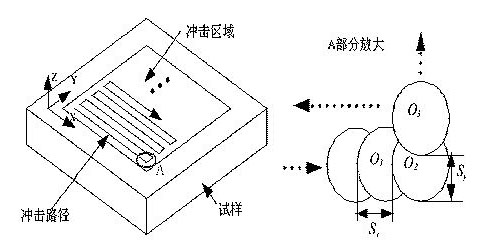
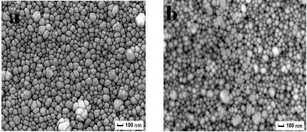
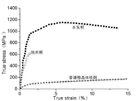
The invention relates to nanocrystal metal materials, in particular to a high-strength high-conductivity nanocrystal copper material and a preparation method thereof. An electrodeposited nano metal copper material is subjected to laser shock treatment at room temperature, wherein laser shock parameters are that: the impulse frequency is 5ns, the shock power is 60-80mJ, the spot size is 2mm, the wavelength is 1,064nm, the selected coating is an aluminum foil with the thickness of 15 mu m, and a restraint layer is made of K9 glass; and an overlapping shock treatment method is adopted, the overlapping rate is 33 percent and the strain rate is 1*10<-6>-1*10<-7> / s. For the nanocrystal copper material prepared by the method, the hardness is improved by 36 to 55 percent, the elastic modulus is improved by 60 to 207 percent, the comprehensive mechanical properties are greatly improved, and the resistivity rho is reduced from 1.52-1.58 to 1.34-1.38 correspondingly, and the nanocrystal copper material can simultaneously meet the requirements on high strength and high conductivity.

Description

technical field [0001] The invention relates to a nanocrystalline metal material, in particular to a high-strength and high-conductivity nanocrystalline copper material and a preparation method thereof. Background technique [0002] Copper and its alloys are still the most widely used metal materials. The main characteristics of copper and its alloys are electrical conductivity and good thermal conductivity (the electrical conductivity and thermal conductivity of pure copper are second only to silver (Ag) among all metal materials), and they have good plasticity and wear resistance. , suitable for various products produced by various plastic processing and casting methods, and is an indispensable metal material in industrial sectors such as electric power, electrician, thermal engineering, chemical industry, instrumentation, shipbuilding and machinery manufacturing. [0003] For pure copper, it has high deformation ability and low strength. Therefore, in order to improve th...

Claims


Application Information

Patent Timeline
IPC IPC(8): C23C14/35C23C14/16C23C14/58B82Y30/00B82Y40/00
Inventor 花银群陈瑞芳
Owner JIANGSU UNIV
Learn More