Radio frequency laterally diffused metal oxide semiconductor (LDMOS) device based on silicon on insulator (SOI) and method for injecting device

A device and radio frequency technology, applied in the field of radio frequency power devices, can solve the problems of poor anti-total dose radiation anti-single event radiation, low power density, low intermodulation distortion performance, etc., to achieve wide application range, improve yield, optimize Effect of on-resistance

CN102054845BActive Publication Date: 2012-11-21BEIJING ZHONGKE XINWEITE SCI & TECH DEV
0 Cites 0 Cited by

Patent Information

Authority / Receiving Office
CN · China
Patent Type
Patents(China)
Current Assignee / Owner
Publication Date
2012-11-21

Smart Images

  • Figure 1
    Figure 1
  • Figure 2
    Figure 2
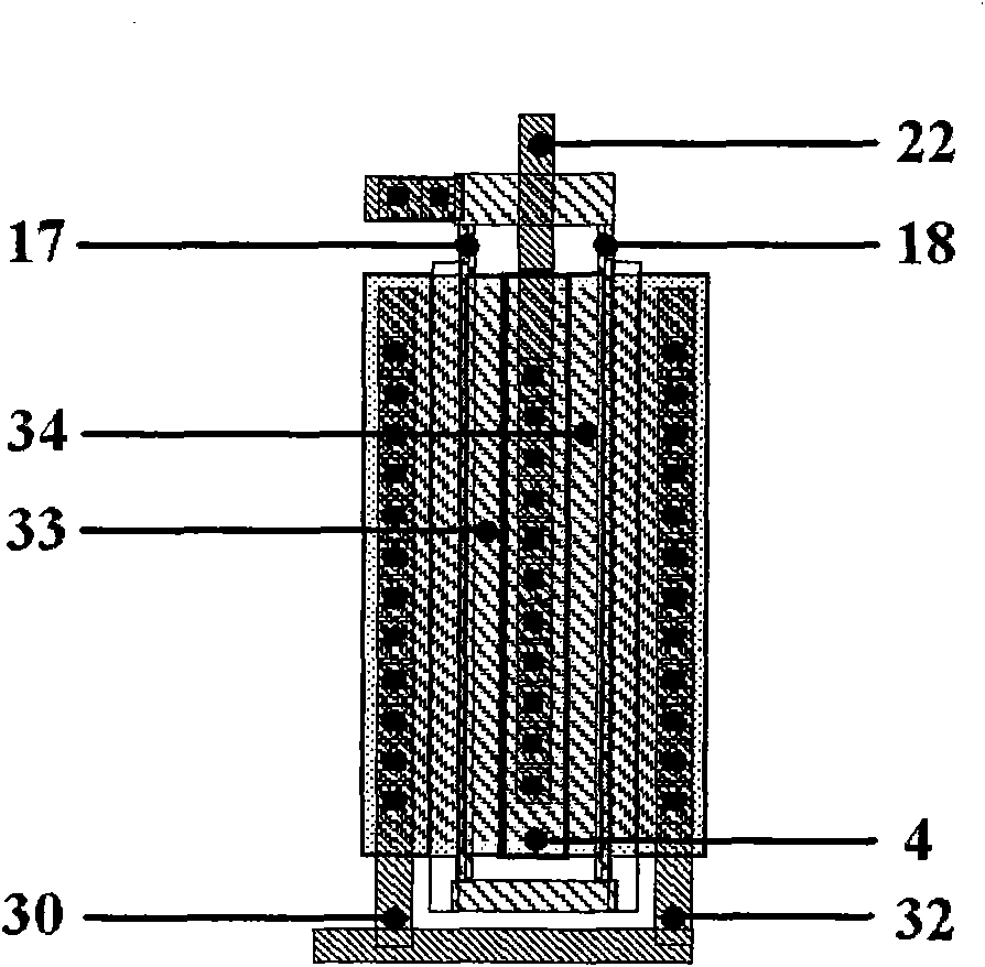
  • Figure 3
    Figure 3
Patent Text Reader

Abstract

The invention discloses a radio frequency silicon on insulator(SOI) laterally diffused metal oxide semiconductor (LDMOS) device provided with a low potential barrier body lead-out, which comprises a bottom layer silicon, a concealed oxide layer, a top layer silicon, a P-region, a N-region, a gate oxide layer, a polysilicon gate layer, a gate polycrystalline silicon carbide layer, a gate electrode, a side wall, a N-drift region, a drain region, a drain region silicate layer, a leakage electrode, a source region, a low potential barrier body lead-out region, a body region, a source region silicide layer, and a source electrode. In the invention, the radio frequency LDMOS device is manufactured on an SOI substrate, and a low potential barrier body lead-out is in a short circuit with the source region is formed by utilizing a heavily doped region homotypic with the P- region; the source / body, leakage / body as well as a gate is interconnected with each electrode by utilizing a silicide; a plurality of grate bars are in interdigital type parallel connection so as to enlarge the driving power of the device; and the invention provides a method for rectifying, back gate injection, N-regioninjection as well as N-drift region injection compatible with a complementary metal-oxide-semiconductor (CMOS) technology, as well as a N-drift region silicide conceal method compatible with the CMOStechnology.
Need to check novelty before this filing date? Find Prior Art

Description

technical field

[0001] The invention relates to the technical field of radio frequency power devices, in particular to a radio frequency SOI LDMOS device with low potential barrier body extraction and a method for injecting it. Background technique

[0002] Laterally Diffused Metal Oxide Semiconductor (LDMOS) process technology (Laterally Diffused Metal Oxide Semiconductor, LDMOS) is mainly for RF power amplifiers of mobile phone base stations in the early stage, due to its high sensitivity, high efficiency, high gain, low distortion, low noise, low thermal resistance, stable frequency , low intermodulation distortion performance and strong automatic gain control capabilities, LDMOS devices are widely used in CDMA, W-CDMA, TETRA, digital terrestrial television and other fields that require wide frequency range, high linearity and high service life, but LDMOS It also has its own limitations, such as low power density, anti-ESD, anti-total dose radiation and poor ability to re...

Examples

Embodiment Construction

[0051] In order to make the object, technical solution and advantages of the present invention clearer, the present invention will be described in further detail below in conjunction with specific embodiments and with reference to the accompanying drawings.

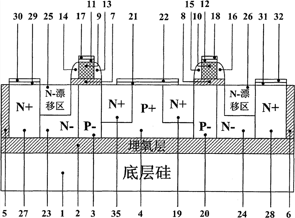
[0052] Such as figure 1 as shown, figure 1 It is a schematic structural diagram of a radio frequency SOILDMOS device with a low barrier body extraction provided by the present invention. The LDMOS device uses a silicon-on-insulator SOI with a top layer of silicon 3, a buried oxide layer 2 and a bottom layer of silicon 1 from top to bottom as the basic structure, This RF LDMOS device consists of:

[0053] P placed on the upper surface of the buried oxide layer - District 20, in the immediate vicinity of P - The first N - District 23 and 2nd N - District 24;

[0054] A first gate oxide layer 7 and a second gate oxide layer 8 disposed on the upper surface of the top silicon layer 3;

[0055] The first polysilicon gate...