Monolithic integrated SiC MEMS (Micro-Electro-Mechanical Systems) pressure sensor and production method thereof

A pressure sensor, monolithic integration technology, applied in the field of micro-electromechanical systems, can solve problems such as inability to apply to corrosive environments, and achieve the effects of reducing packaging costs, improving accuracy and stability, and high gain

Inactive Publication Date: 2011-05-18
PEKING UNIV
View PDF5 Cites 38 Cited by
  • Summary
  • Abstract
  • Description
  • Claims
  • Application Information

AI Technical Summary

Problems solved by technology

[0005] So far, many commercially available pressure sensors are mostly silicon-based, which cannot be used in cor

Method used


Image

  • Monolithic integrated SiC MEMS (Micro-Electro-Mechanical Systems) pressure sensor and production method thereof
  • Monolithic integrated SiC MEMS (Micro-Electro-Mechanical Systems) pressure sensor and production method thereof
  • Monolithic integrated SiC MEMS (Micro-Electro-Mechanical Systems) pressure sensor and production method thereof

Examples


Embodiment 1

[0048] Embodiment 1 Preparation of capacitive pressure sensor

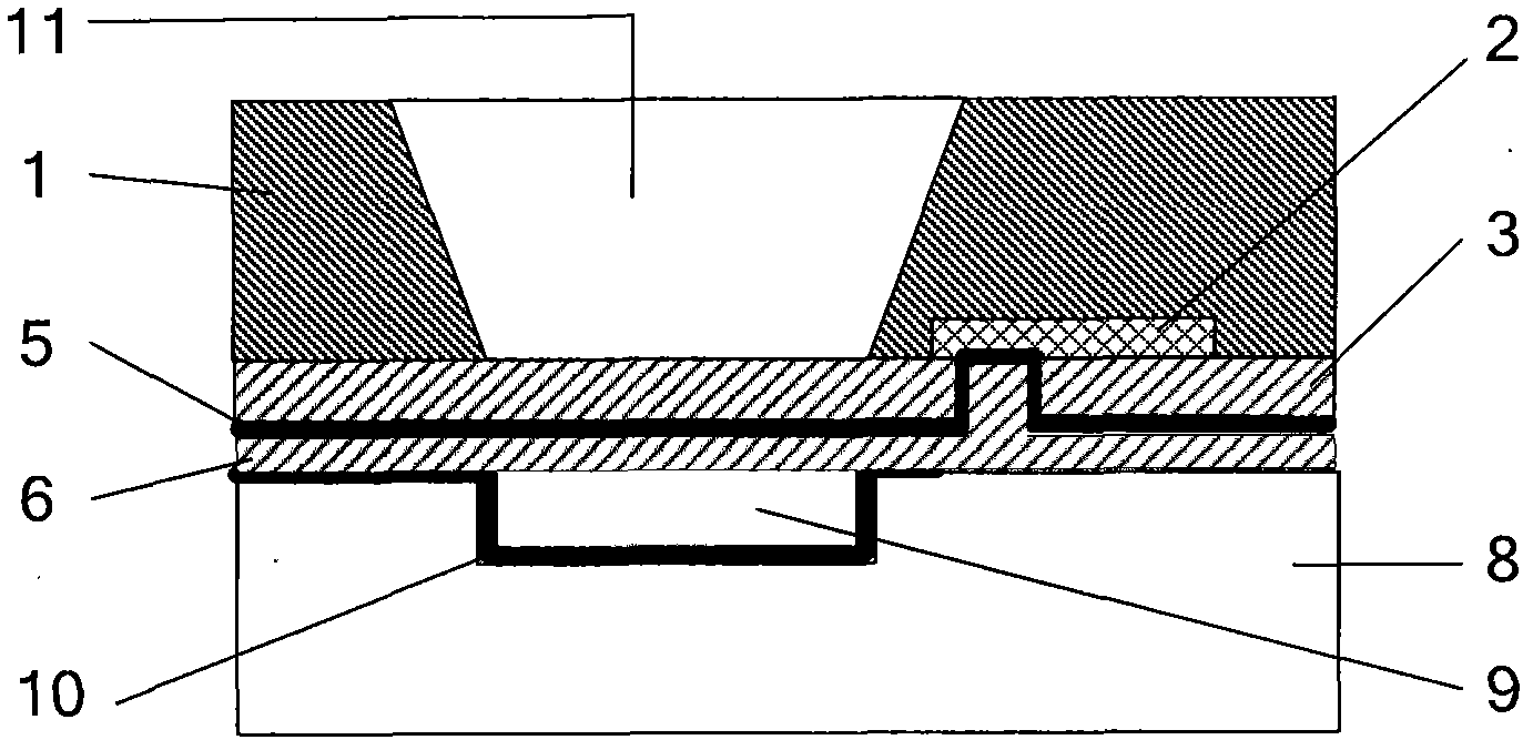
[0049] Raw materials: double-sided polished N-type silicon wafer 10, resistivity 2-4 Ω-cm, crystal orientation , silicon wafer thickness 400 μm; 7740 glass.

[0050] Such as figure 1 As shown, the monolithic integrated capacitive pressure sensor includes a silicon wafer 1 as the first substrate, a CMOS processing circuit 2, a SiC thin film 3 as the structural layer, an upper electrode 5, a SiC thin film 6 as the dielectric layer, and a second SiC thin film as the second substrate. The glass 8 of the substrate, the lower electrode 10, and the pressure chamber 9 and the deep groove 11, its preparation process is as follows:

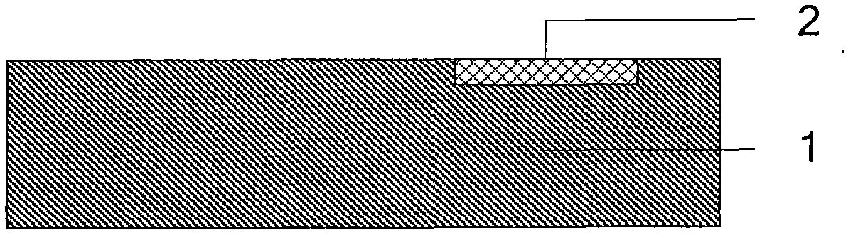
[0051] 1. Manufacturing a CMOS processing circuit 2 on a silicon wafer 1 with a CMOS process, such as Figure 2a shown.

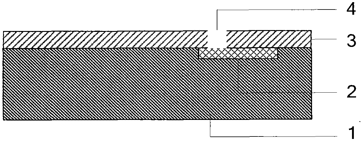
[0052] 2. Deposit a SiC thin film 3 with a thickness of 0.2 μm to 5 μm on the silicon wafer 1 by using PECVD (plasma enhanced chemical vapor deposition) technology, and ...

Embodiment 2

[0062] We first use the BD031 integrated circuit (such as Figure 6 shown) to test the performance of the device part (excluding the CMOS processing circuit) of the above-mentioned integrated pressure sensor. This IC is based on a switched capacitor network to convert capacitance to voltage. Figure 6 In, Vout is the output signal, V B is the reference voltage of 2.25 volts, C1 and C2 are the input capacitors, where C1 is the sensor capacitor, C2 is the fixed capacitor, C F is the feedback capacitor.

[0063] Connect the BD031 integrated circuit and the sensor into the pressure chamber through the PCB (printed circuit board), use the commercial PPC2+ pressure calibrator to control the air pressure in the pressure chamber, and use the Agilent 34401A multimeter to measure the voltage change. The computer is connected to control the real-time performance of the voltage data and air pressure data. The measurement temperature is between 25°C and 125°C, and the loading pressure ...

Embodiment 3

[0066] based on Figure 4 We have designed a set of test schemes for the entire integrated sensor (device part and CMOS processing circuit) for the bridge connection method of the capacitor shown, and the specific function is to convert different capacitance signals into voltage signals. The schematic diagram of the circuit is as image 3 shown. Some external components are connected to the integrated sensor through the PCB board. Also tested with PPC2+ pressure calibrator and Agilent 34401A multimeter.

[0067] Figure 8 is the measurement result at room temperature. Depend on Figure 8 It can be seen that the data between 110kPa and 300kPa has a good linearity, the linearity between them is 4.0%, and the sensitivity is 0.1585mV / kPa.


PUM

PropertyMeasurementUnit
Thicknessaaaaaaaaaa
Sensitivityaaaaaaaaaa

Abstract

The invention discloses a monolithic integrated SiC MEMS (Micro-Electro-Mechanical Systems) pressure sensor and a production method thereof. The pressure sensor comprises a first substrate in which a CMOS (Complementary Metal Oxide Semiconductor) processing circuit is inlayed, a second substrate provided with a pressure cavity and a capacitor induction thin film arranged between the two substrates. The thin film is formed sandwiching an electrode between two layers of PECVD SiC thin films and is suspended on the pressure cavity; a lower electrode covers the surface of the pressure cavity; part of the first substrate above the pressure cavity is provided with a deep groove for exposing the PECVD SiC thin film on the upper layer; the CMOS processing circuit is located beside the deep groove and is communicated with the upper electrode. The sensor uses SiC of low-temperature deposition as the induction thin film, has good performance and is suitable for corrosive environment. Besides, the invention realizes integration between the sensor and the processing circuit by using a post-CMOS method so as to improve the integral precision and stability of the device.

Description

technical field [0001] The invention relates to an integration scheme of a SiC MEMS capacitive pressure sensor and a readout circuit thereof, belonging to the field of micro-electromechanical systems. Background technique [0002] In recent years, with the continuous development and maturity of MEMS (Micro-Electro-Mechanical Systems) technology, various MEMS devices and systems have shined brilliantly in the fields of automobiles, consumer electronics, biomedical and other fields, and have become a research field in high-tech fields. Hotspots and new forces in the industry have gained widespread attention. And silicon-based MEMS has achieved great success. [0003] Pressure sensor is one of the most successful products of MEMS, and it has been widely used in automobile, industrial processing, medical treatment and aerospace. However, in recent years, due to the limitations of the characteristics of silicon materials, silicon-based devices are difficult to apply in high-tem...

Claims


Application Information

Patent Timeline
IPC IPC(8): G01L9/12B81B7/00B81C1/00
Inventor 唐伟陈哲郑百祥刘雷张海霞
Owner PEKING UNIV
Why Eureka
Try Eureka