Manufacturing method for surface roughening of GaN-based optoelectronic device

A surface roughening and electronic device technology, which is applied in the field of p-type layer roughening on the surface of photoelectric conversion devices, can solve the problem of reducing the conductivity type of the p-GaN layer, increasing the contact resistance between the electrode and the p-GaN, and the roughening effect is not ideal. and other problems, to achieve the effect of less surface defects and less chance of reflection

Inactive Publication Date: 2011-05-18
INST OF SEMICONDUCTORS - CHINESE ACAD OF SCI
View PDF0 Cites 5 Cited by
  • Summary
  • Abstract
  • Description
  • Claims
  • Application Information

AI Technical Summary

Problems solved by technology

At present, there are two main methods for roughening the surface of GaN-based optoelectronic devices, which are mainly produced in the process of GaN-based LED devices: one is to roughen the surface of GaN-based LEDs after the epitaxial growth is completed. The existing methods include Use wet etching or dry etching to roughen the surface of the p-GaN layer, but this method will cause etching damage to the p-GaN surface, thereby increasing the contact resistance between the electrode and p-GaN
Another method is to directly grow a rough p-GaN layer. Usually, the surface of the p-GaN layer is roughened by low growth temperature or heavy doping of Mg. However, this method will introduce many defects in the p-GaN layer. Reduce the conductivity type of the p-GaN layer, and the roughening effect is not ideal

Method used


Image

  • Manufacturing method for surface roughening of GaN-based optoelectronic device
  • Manufacturing method for surface roughening of GaN-based optoelectronic device
  • Manufacturing method for surface roughening of GaN-based optoelectronic device

Examples


Embodiment 1

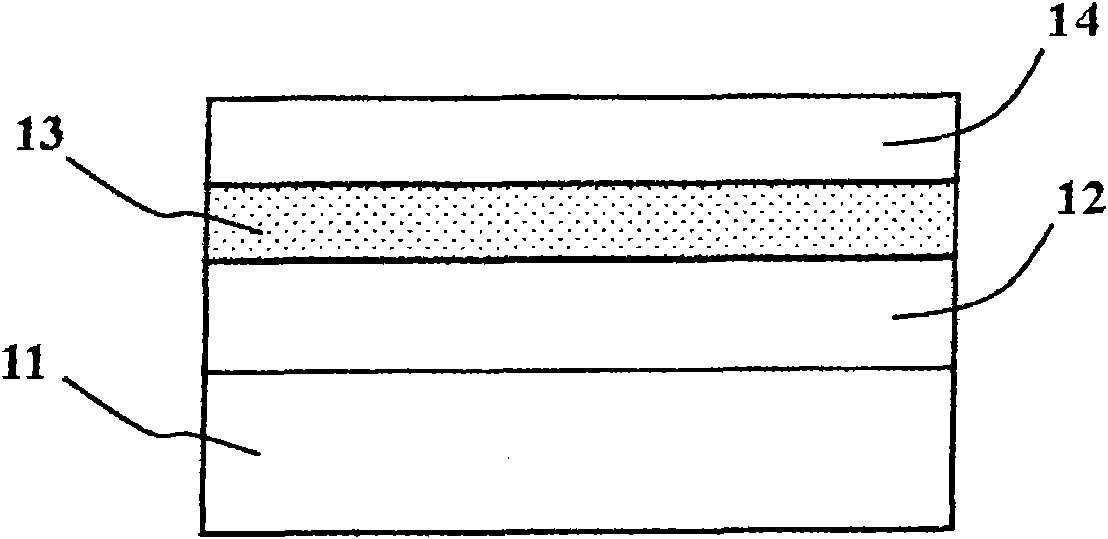
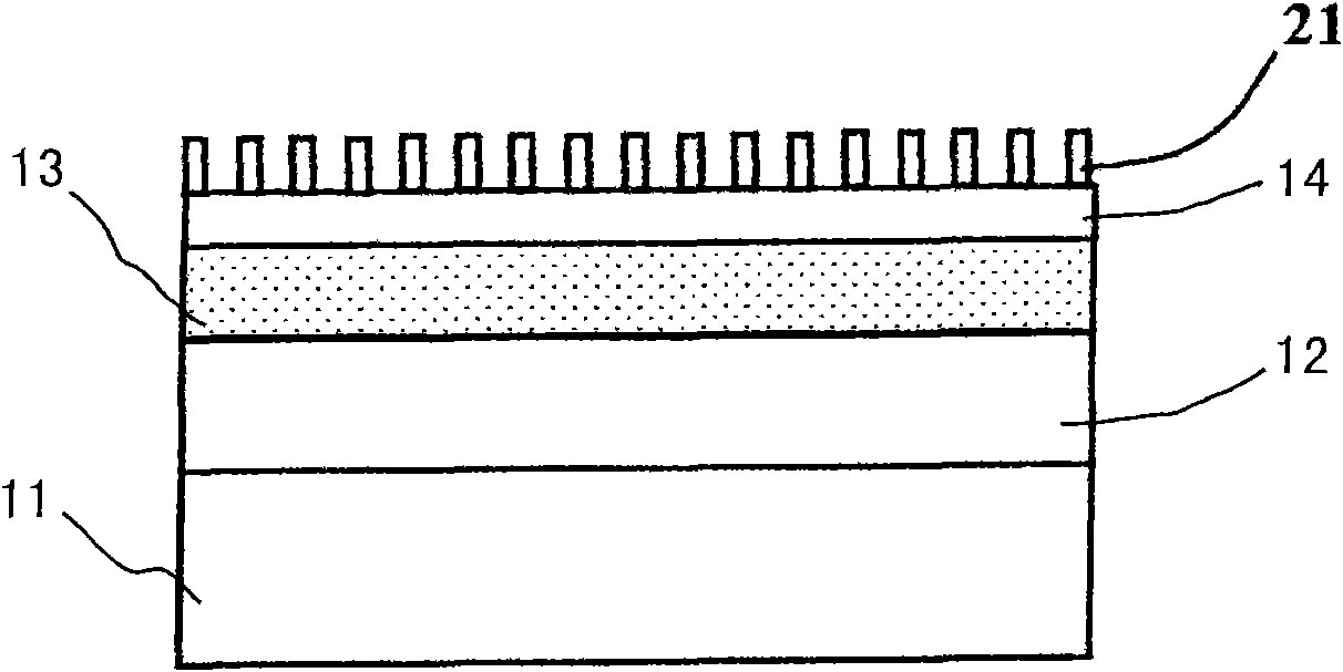
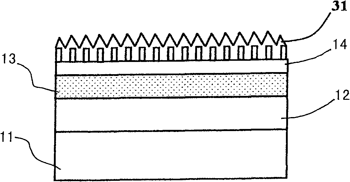
[0036] Embodiment one: see Figure 1-Figure 3 shown. Use Metal Organic Chemical Vapor Deposition (MOCVD) method to epitaxially grow n-type layer 12, i-type layer 13, p-type layer 14 sequentially on substrate 11, wherein said substrate 11 is a sapphire substrate; n-type layer 12 is The n-type GaN epitaxial layer has a thickness of 3000nm; the i-type layer 13 is In 0.1 Ga 0.9 N / GaN multi-quantum well structure with a thickness of 60nm; the p-type layer 14 is a p-type GaN material with a thickness of 150nm; then deposit 200nm thick SiO on the p-type layer 14 2 Dielectric film; then in SiO 2 A layer of metal Ni is evaporated on the dielectric film, and the metal Ni is aggregated into metal islands with a diameter of about 10-200 nanometers by means of rapid annealing. Use the metal island as a mask material to etch the p-type layer 14 with an etching depth of 100nm, thereby producing the nano-column array 21; then, grow the p-type thick p-type layer on the surface of the epita...

Embodiment 2

[0037] Embodiment two: see Figure 1-Figure 3 shown. Use metal organic chemical vapor deposition (MOCVD) method to epitaxially grow n-type layer 12, i-type layer 13, p-type layer 14 sequentially on substrate 11, wherein said substrate 11 is n-type GaN substrate material; n-type Layer 12 is an n-type GaN epitaxial layer with a thickness of 300nm; the i-type layer 13 is In 0.1 Ga 0.9 N / GaN multi-quantum well structure with a thickness of 60nm; the p-type layer 14 is a p-type GaN material with a thickness of 150nm; then deposit 200nm thick SiO on the p-type layer 14 2 Dielectric film; then in SiO 2 A layer of metal Ni is evaporated on the dielectric film, and the metal Ni is aggregated into metal islands with a diameter of about 10-200 nanometers by means of rapid annealing. Use the metal island as a mask material to etch the p-type layer 14 with an etching depth of 100nm, thereby producing the nano-column array 21; then, grow the p-type thick p-type layer on the surface of t...

Embodiment 3

[0038] Embodiment three: see Figure 1-Figure 3 shown. Use Metal Organic Chemical Vapor Deposition (MOCVD) method to epitaxially grow n-type layer 12, i-type layer 13, p-type layer 14 sequentially on substrate 11, wherein said substrate 11 is a sapphire substrate; n-type layer 12 is The n-type GaN epitaxial layer has a thickness of 3000nm; the i-type layer 13 is intrinsic In 0.2 Ga 0.8 N layer with a thickness of 200nm; the p-type layer 14 is a p-type GaN material with a thickness of 150nm; then deposit 200nm thick SiO on the p-type layer 14 2 Dielectric film; then in SiO 2 A layer of metal Ni is evaporated on the dielectric film, and the metal Ni is aggregated into metal islands with a diameter of about 10-200 nanometers by means of rapid annealing. Use the metal island as a mask material to etch the p-type layer 14 with an etching depth of 100nm, thereby producing the nano-column array 21; then, grow the p-type thick p-type layer on the surface of the epitaxial wafer wit...


PUM

PropertyMeasurementUnit
thicknessaaaaaaaaaa
thicknessaaaaaaaaaa
thicknessaaaaaaaaaa

Abstract

The invention discloses a manufacturing method for surface roughening of a GaN-based optoelectronic device, which comprises the following steps of: 1, taking a substrate; 2, epitaxially growing an n-type layer, an i-type layer and a p-type layer in turn on the substrate; 3, processing a nano column array on the p-type layer by using nano processing technology; and 4, epitaxially growing a p-type surface roughened layer on the nano column array.

Description

technical field [0001] The invention relates to a process for roughening the surface of an optoelectronic device, in particular to a method capable of roughening the p-type layer on the surface of GaN-based LEDs and other electro-optic conversion devices and solar cells and other photo-electric conversion devices. Background technique [0002] Group III nitride semiconductor materials represented by GaN have broad application prospects in the fields of optoelectronics and microelectronics. The forbidden band width of GaN, InN, AlN and their alloy materials (such as InGaN, AlGaN) with direct bandgap covers the wavelength band from infrared to ultraviolet, which can be used to make light-emitting diodes (LEDs), high-performance ultraviolet detectors, purple and blue-green light Lasers (LD), high-efficiency solar cells, etc., are widely used in fields such as full-color display, white light illumination, high-density information storage, laser printing, underwater communication...

Claims


Application Information

Patent Timeline
Patent Type & Authority Applications(China)
IPC IPC(8): H01L33/22H01L31/18H01L31/0236
CPCY02E10/50Y02P70/50
Inventor 王辉朱建军张书明杨辉
Owner INST OF SEMICONDUCTORS - CHINESE ACAD OF SCI
Why Eureka
Try Eureka