Solar battery cell and process for producing the same

一种太阳能电池、制造方法的技术,应用在电气元件、最终产品制造、可持续制造/加工等方向,能够解决工序数增加、无法高效地量产太阳能电池单元等问题,达到制造工序简化、电池单元特性优良、廉价制作的效果

Inactive Publication Date: 2011-05-25
MITSUBISHI ELECTRIC CORP
View PDF1 Cites 24 Cited by
  • Summary
  • Abstract
  • Description
  • Claims
  • Application Information

AI Technical Summary

Problems solved by technology

In this way, when a silicon oxide film is used in the back passivation film, it is necessary to form a resist pattern in the back passivation film by photolithography, and to open the silicon oxide film with hydrofluoric acid. , the number of processes has also increased significantly, making it impossible to efficiently mass-produce solar cells

Method used


Image

  • Solar battery cell and process for producing the same
  • Solar battery cell and process for producing the same
  • Solar battery cell and process for producing the same

Examples


Embodiment approach 1

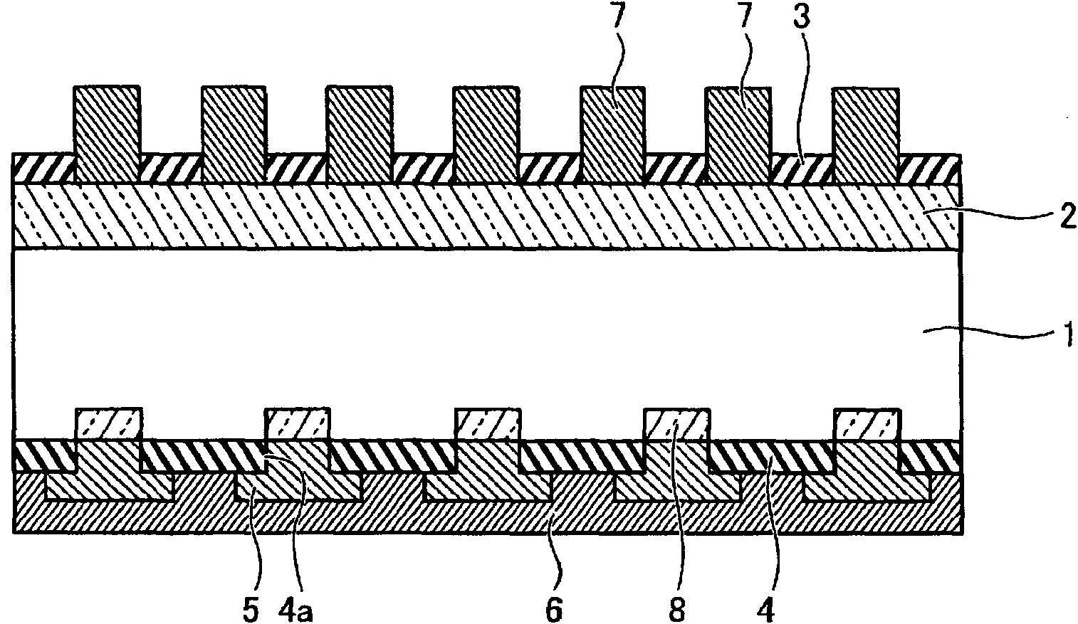
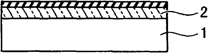
[0061] figure 1 It is a cross-sectional view for explaining the structure of the solar cell according to Embodiment 1 of the present invention. In the solar cell of this embodiment, on the light-receiving surface side of the semiconductor substrate 1 made of p-type silicon, the impurity diffusion layer (n-type impurity diffusion layer) 2 is formed by diffusion of phosphorus, and the silicon nitride film is formed. The antireflection film 3 constituted.

[0062] As the semiconductor substrate 1, a p-type single crystal or polycrystalline silicon substrate can be used. In addition, the substrate is not limited thereto, and an n-type silicon substrate may also be used. In addition, a silicon oxide film may also be used for the antireflection film 3 . In addition, on the light-receiving surface side surface of the semiconductor substrate 1 of the solar battery cell, fine unevenness is formed as a texture structure. The micro-concave-convex is a structure that increases the are...

Embodiment approach 2

[0081] In Embodiment 2, another solar battery cell and its manufacturing method of the present invention will be described in detail. Figure 4 It is a sectional view for explaining the structure of the solar cell of Embodiment 2 of this invention. In addition, in the following drawings, with respect to the same structure as Embodiment 1, by adding and figure 1 The same symbols are used, and detailed explanations are omitted.

[0082] In the solar cell of this embodiment, on the light-receiving surface side of the semiconductor substrate 1 made of p-type silicon, an impurity diffusion layer (n-type impurity diffusion layer) 2 is formed by diffusion of phosphorus and a silicon nitride film is formed. anti-reflection film 3. On the light-receiving surface side surface of the semiconductor substrate 1 of the solar battery cell, fine unevenness is formed as a texture structure. The micro-concave-convex is a structure that increases the area that absorbs light from the outside o...


PUM


Abstract

A second conductivity type impurity diffusion layer and an antireflection film are formed on one side of a first conductivity type semiconductor substrate. A glass-containing first electrode material is coated on the antireflection film. A passivation film is formed on the other side of the semiconductor substrate. A plurality of opening parts, which reaches the other side of the semiconductor substrate, is formed in at least a part of the passivation film. A second electrode material containing the first conductivity type impurity element is coated so as to embed the plurality of opening parts and so as not to come into contact with the second electrode material in the adjacent opening part. A third electrode material is coated onto the passivation film so as to come into contact with the coated whole second electrode material. After coating the first electrode material and the third electrode material, the semiconductor substrate is heated at a predetermined temperature. The above constitution can realize simultaneous formation of a first electrode, which passes through the antireflection film and is electrically connected to the impurity diffusion layer, a high-concentration region, in which, on the other side of the semiconductor substrate, the first conductivity type impurity is diffused in a higher concentration than the other region of the semiconductor substrate, and the second and third electrodes electrically connected to the high-concentration region.

Description

technical field [0001] The present invention relates to a solar battery cell and a method for manufacturing the same, and particularly to a solar battery cell capable of reducing warping of the solar cell and having good characteristics even when the substrate is thinned, and such a solar cell that can be efficiently manufactured A method of manufacturing a unit solar cell unit. Background technique [0002] Conventionally, aluminum pastes used as rear aluminum electrodes of photovoltaic devices such as solar cells have an advantage that the electrodes can be easily formed by methods such as screen printing. In addition, the aluminum paste has an advantage that a so-called BSF (Back Surface Field: Back Surface Field) layer can be easily formed, that is, a layer in which aluminum is diffused into a silicon substrate and a p-type impurity is diffused at a high concentration can be easily formed by heat treatment. p+ layer, and generate a barrier electric field for the minorit...

Claims


Application Information

Patent Timeline
Patent Type & Authority Applications(China)
IPC IPC(8): H01L31/04
CPCH01L31/1804H01L31/02245H01L31/068H01L31/022425H01L31/0682Y02E10/50Y02E10/547H01L31/02167H01L31/0504Y02P70/50
Inventor 滨笃郎森川浩昭
Owner MITSUBISHI ELECTRIC CORP
Why Eureka
Try Eureka