MIS capacitor lower piezoresistance structure adopting substrate grid and making method

A manufacturing method and substrate gate technology, applied in the field of sensors, can solve problems such as increasing the difficulty of the process, achieve the effects of simplifying the structure and process, realizing self-alignment, and avoiding protection

A manufacturing method and substrate gate technology, applied in the field of sensors, can solve problems such as increasing the difficulty of the process, achieve the effects of simplifying the structure and process, realizing self-alignment, and avoiding protection

CN102134052AInactive Publication Date: 2011-07-27SHANGHAI INST OF MICROSYSTEM & INFORMATION TECH CHINESE ACAD OF SCI

Image

  • MIS capacitor lower piezoresistance structure adopting substrate grid and making method
  • MIS capacitor lower piezoresistance structure adopting substrate grid and making method
  • MIS capacitor lower piezoresistance structure adopting substrate grid and making method

Examples


Embodiment Construction

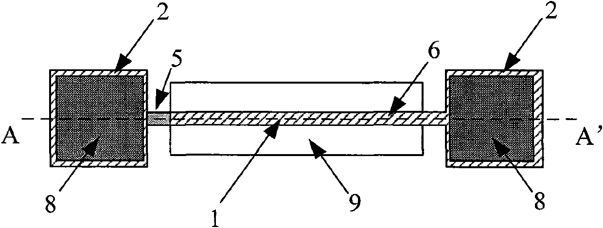
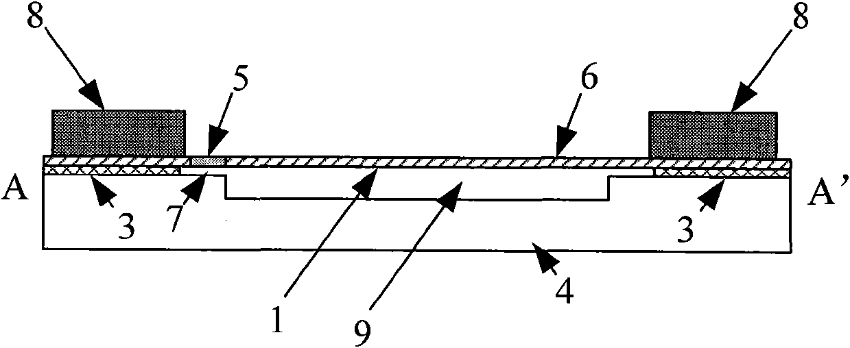
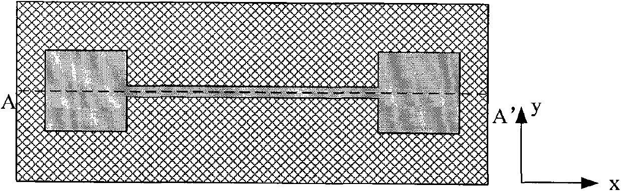
[0028] The piezoresistive structure under the MIS capacitance of the substrate gate is used to detect the displacement of the nano-beam. The structure includes a nano-beam 1 made of the top silicon of the SOI silicon wafer; the nano-beam is provided with a doped region, including lightly doped The impurity region 5 and the heavily doped region 6 located at both ends of the lightly doped region; the bottom of the two ends of the nanobeam is fixed on the silicon substrate 4 through the oxide layer 3, and freely vibrates in the z direction; the lightly doped region and A gap 7 is provided between the silicon substrates; a pressure welding block 8 is provided on the heavily doped regions at both ends of the nano-beam.

[0029] The nanobeam mentioned in the present invention refers to a beam structure with a thickness less than 100 nanometers. Figure 1a -1c shows the cross-sectional view of the substrate electrode and the double-terminal fixed-supported nanobeam structure. The na...


PUM

PropertyMeasurementUnit
thicknessaaaaaaaaaa

Abstract

The invention relates to a metal insulator semiconductor (MIS) capacitor lower piezoresistance structure adopting a substrate grid and an automatic alignment processing technology for implementing the piezoresistance structure. The structure is used for detecting the displacement of a nano beam. According to the structure, the nano beam is made of top silicon of a silicon on insulator (SOI) chip,a silicon substrate is used as the grid, a silicon dioxide buried layer between the beam and the silicon substrate is removed by corroding to form a clearance, and the silicon substrate, the clearance and the nano beam form the MIS capacitor structure. A voltage is applied to the substrate grid so that a strong inversion layer is formed on the lower surface of the nano beam, and the inversion layer and the silicon above a space charge region are used as piezoresistors to realize piezoresistance detection of vibration of the nano beam. Automatic alignment of a light doped region on the beam and the substrate grid can be realized by combining a composite mask and corrosion of an anisotropic wet method.

Description

technical field [0001] The invention relates to a piezoresistive structure under an MIS capacitor for detecting the displacement of a nanometer beam and a self-alignment processing technology for realizing the piezoresistive structure. In this structure, the silicon substrate under the nanobeam is used as the gate, and the MIS capacitor is formed with the nanobeam. The space charge region formed by the MIS capacitor is used to change the symmetry of the nanobeam carrier to form a force sensitive resistor, and the nanometer is detected by the piezoresistive effect. beam displacement. It belongs to the field of sensors. Background technique [0002] Nano Electro Mechanical System (NEMS) technology is the use of integrated circuit technology to form a nanoscale structure on a silicon wafer to realize the technology of sensors and actuators (K.L.Ekinci, M.L.Roukes.Nanoelectromechanical systems.Review of Scientific Instruments, Vol.76, 061101, 2005.). [0003] Beam structures ...

Claims


Application Information

Patent Timeline
27 Jul 2011
Publication
CN102134052A
IPC
B81B7/02; B81C1/00; G01L1/18
Inventors
杨恒; 吴燕纒