Method for preparing single-layer graphene
A single-layer graphene and graphene technology, applied in the field of two-dimensional thin film material preparation, can solve problems such as methods that are not suitable for large-scale preparation and application of industrial production, difficult to reuse, and expensive for single-crystal metal substrates. The effect of controllable growth of mass and large area and uniform distribution of layers
- Summary
- Abstract
- Description
- Claims
- Application Information
AI Technical Summary
Problems solved by technology
Method used
Image
Examples
Embodiment 1
[0035] Embodiment 1, preparation monolayer graphene
[0036] 1) Select a molybdenum foil with a thickness of 200 μm as the metal substrate, and use the electron beam evaporation method, in a vacuum of 1×10 -7 mbar, a polycrystalline nickel film with a thickness of 200nm is vapor-deposited on the molybdenum foil metal substrate at a temperature of 25°C to obtain an alloy substrate;
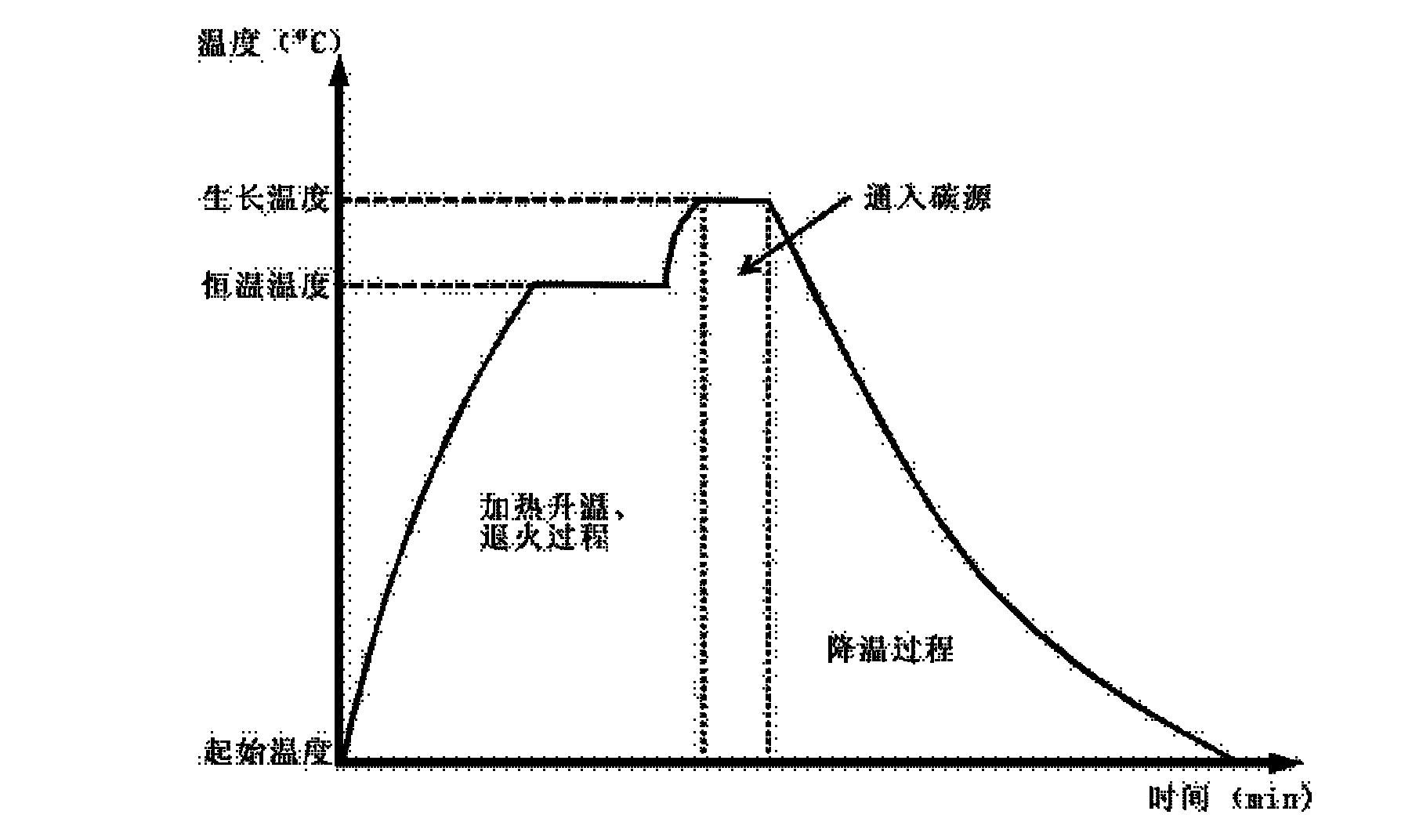
[0037] 2) In hydrogen gas (flow rate of 400 sccm) and argon gas (flow rate of 500 sccm), the alloy substrate obtained in step 1) was heated from room temperature to 900° C. for 25 minutes in a tube furnace, then annealed at a constant temperature for 20 minutes, and then subjected to Heat up to the catalytic growth temperature of 1000° C. in 5 minutes. At this time, feed carbon source methane (flow rate is 50 sccm) and stay for 5 minutes to grow. The volume ratio of methane gas to hydrogen gas is 16:1, and then 15° C. / min The cooling rate is reduced to 700°C, the heater is turned off, and the temp...
Embodiment 2
[0044] Embodiment 2, prepare single-layer graphene (thinning the thickness of metal substrate to 1 / 8 of embodiment 1, increasing the carbon source concentration to 8 times of embodiment 1 during growth, extending the growth time to 6 times of embodiment 1)
[0045] 1) Select a molybdenum foil with a thickness of 25 μm as the metal substrate, and use the electron beam evaporation method, in a vacuum of 1×10 -7 mbar, a polycrystalline nickel film with a thickness of 200nm is vapor-deposited on the molybdenum foil metal substrate at a temperature of 25°C to obtain an alloy substrate;
[0046] 2) In hydrogen gas (flow rate of 400 sccm) and argon gas (flow rate of 500 sccm), the alloy substrate obtained in step 1) was heated from room temperature to 900° C. for 25 minutes in a tube furnace, then annealed at a constant temperature for 20 minutes, and then subjected to Heat up to the catalytic growth temperature of 1000° C. in 5 minutes. At this time, feed carbon source methane (flow...
Embodiment 3
[0049] Embodiment 3, prepare single-layer graphene (thinning the thickness of metal substrate to 1 / 8 of embodiment 1, increase the carbon source concentration to 8 times of embodiment 1 during growth, reduce the cooling rate to 1 / 8 of embodiment 1 4)
[0050] 1) Select a molybdenum foil with a thickness of 25 μm as the metal substrate, and use the electron beam evaporation method, in a vacuum of 1×10 -7 mbar, a polycrystalline nickel film with a thickness of 200nm is vapor-deposited on the molybdenum foil metal substrate at a temperature of 25°C to obtain an alloy substrate;
[0051] 2) In hydrogen gas (flow rate of 400 sccm) and argon gas (flow rate of 500 sccm), the alloy substrate obtained in step 1) was heated to 900°C in a tube furnace, then annealed at a constant temperature for 20 minutes, and then heated to a catalytic growth temperature of 1000°C At this time, the carbon source methane (flow rate is 50sccm) is passed through for 5 minutes to grow, the volume ratio of...
PUM
| Property | Measurement | Unit |
|---|---|---|
| Thickness | aaaaa | aaaaa |
Abstract
Description
Claims
Application Information


