Method for preparing graphical GaN substrate
A patterning and substrate technology, applied in semiconductor/solid-state device manufacturing, electrical components, circuits, etc., can solve problems such as poor thermal conductivity and large lattice mismatch, and achieve improved light extraction efficiency and thermal conductivity, excellent Performance, the effect of improving luminous efficiency
- Summary
- Abstract
- Description
- Claims
- Application Information
AI Technical Summary
Problems solved by technology
Method used
Image

Examples
Embodiment 1
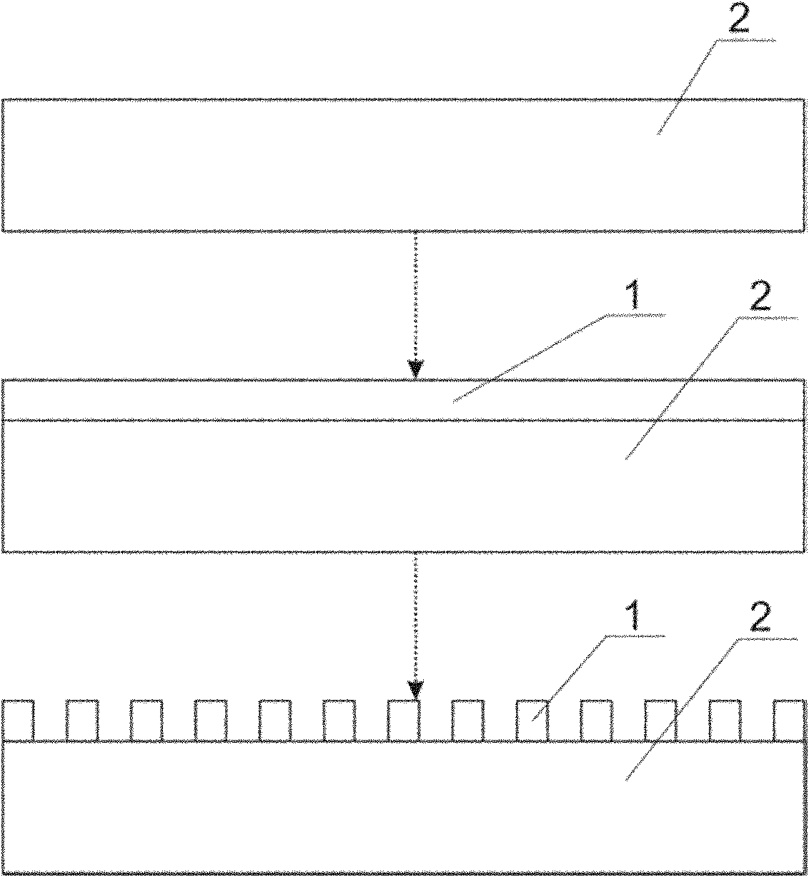
[0026] Step exposure method plus dry etching technology (GaN single crystal substrate 2)
[0027] 1. Select a 2-inch GaN single crystal substrate with a thickness of 300 microns;
[0028] 2. Use a coating machine to coat a photoresist 1 with a thickness of 3 microns on the surface of the above-mentioned GaN single crystal, see attached figure 1 The second step shows the coating of 3 micron thick photoresist 1 and 300 micron thick GaN single crystal substrate 2;
[0029] 3. Expose the GaN single crystal substrate coated with 3 micron photoresist through a step exposure machine, and form a cylindrical pattern with a surface period of 3 microns after development, as shown in the attached figure 1 The third step shows a 2-inch GaN single crystal substrate with a periodic photoresist pattern after distributed exposure, and a product with a 3 micron periodic photoresist pattern and a 300 micron thick GaN single crystal substrate;
[0030] 4. Put the sample with periodic pattern ph...
Embodiment 2
[0032] Step exposure method plus dry etching technology (GaN / Al 2 o 3 composite substrate)
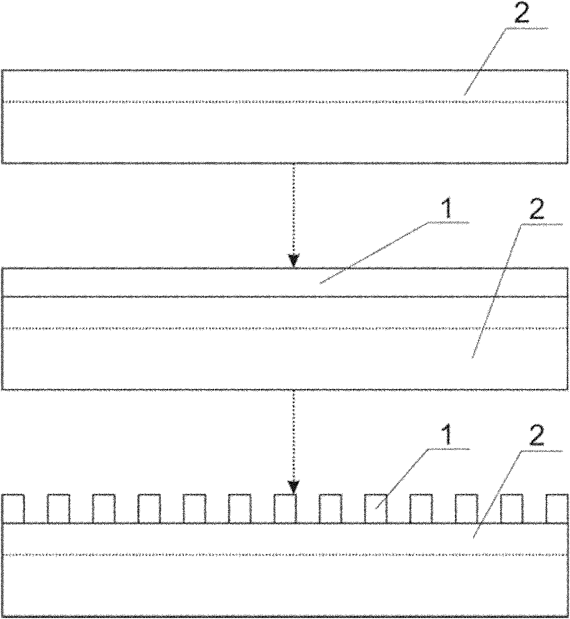
[0033] Select a 2-inch GaN / Al with a thickness of 10 microns GaN and 430 microns sapphire 2 o 3 composite substrate. attached image 3 2-inch GaN / Al with 10 micron GaN, 430 micron sapphire shown in the first step 2 o 3 Composite substrate, composite substrate 2 can be selected with a surface layer of 10 micron GaN and a lower layer of 430 micron sapphire; use a coating machine to coat a photoresist with a thickness of 3 microns on the surface of the above-mentioned GaN single crystal; image 3 Step 2 shows GaN / Al coated with 3 micron photoresist 2 o 3 Composite substrate;
[0034] The GaN single crystal substrate coated with 3 micron photoresist was exposed by a step exposure machine, and developed to form a cylindrical pattern with a surface period of 3 microns, attached image 3 The third step shows a 2-inch GaN single crystal substrate with a periodic photoresist pattern a...
Embodiment 3
[0037] Step exposure wet etching technology (GaN / Al 2 o 3 composite substrate)
[0038] Select a 2-inch GaN / Al with a thickness of 10 microns GaN and 430 microns sapphire 2 o 3 Composite substrate, with Figure 5 2-inch GaN / Al with 10 micron GaN, 430 micron sapphire shown in the first step 2 o 3 Composite substrate, the surface layer is 10 micron GaN, and the lower layer is 430 micron sapphire; PECVD equipment is used to grow silica (SiO2)3 with a thickness of 2 microns on the surface of the above-mentioned GaN single crystal, and attach Figure 5 The second step shows the GaN / Al growth of SiO2 with a thickness of 2 microns 2 o 3 Composite substrate, access to 2 micron silica (SiO2)3 mask, 430 micron GaN / Al 2 o 3 Composite substrate products.
[0039] Utilize photoresist 1 equally, press the step-by-step adhesive development exposure method of embodiment two, in above-mentioned growth 2 micron SiO2 GaN / Al 2 o 3 Cylindrical patterns with a period of 3 micrometers ar...
PUM
| Property | Measurement | Unit |
|---|---|---|
| Thickness | aaaaa | aaaaa |
| Depth | aaaaa | aaaaa |
Abstract
Description
Claims
Application Information
 - R&D
- Intellectual Property
- Life Sciences
- Materials
- Tech Scout
- Unparalleled Data Quality
- Higher Quality Content
- 60% Fewer Hallucinations
Browse by: Latest US Patents, China's latest patents, Technical Efficacy Thesaurus, Application Domain, Technology Topic, Popular Technical Reports.
© 2025 PatSnap. All rights reserved.Legal|Privacy policy|Modern Slavery Act Transparency Statement|Sitemap|About US| Contact US: help@patsnap.com