Separation method of LED (light emitting diode) epitaxy chip

A separation method and epitaxial wafer technology, applied in laser welding equipment, electrical components, circuits, etc., can solve the problems of dust pollution, low efficiency, long time consumption, etc., to simplify separation operations, improve separation efficiency, and reduce production costs. Effect

Active Publication Date: 2011-08-17
SUZHOU NAFANG TECH DEV
View PDF4 Cites 6 Cited by
  • Summary
  • Abstract
  • Description
  • Claims
  • Application Information

AI Technical Summary

Problems solved by technology

In this cutting process, because the thinning and polishing of sapphire, silicon carbide and other substrates are very difficult, time-consuming, inefficient, and easily lead to irregul

Method used


Image

  • Separation method of LED (light emitting diode) epitaxy chip
  • Separation method of LED (light emitting diode) epitaxy chip
  • Separation method of LED (light emitting diode) epitaxy chip

Examples


Embodiment 1

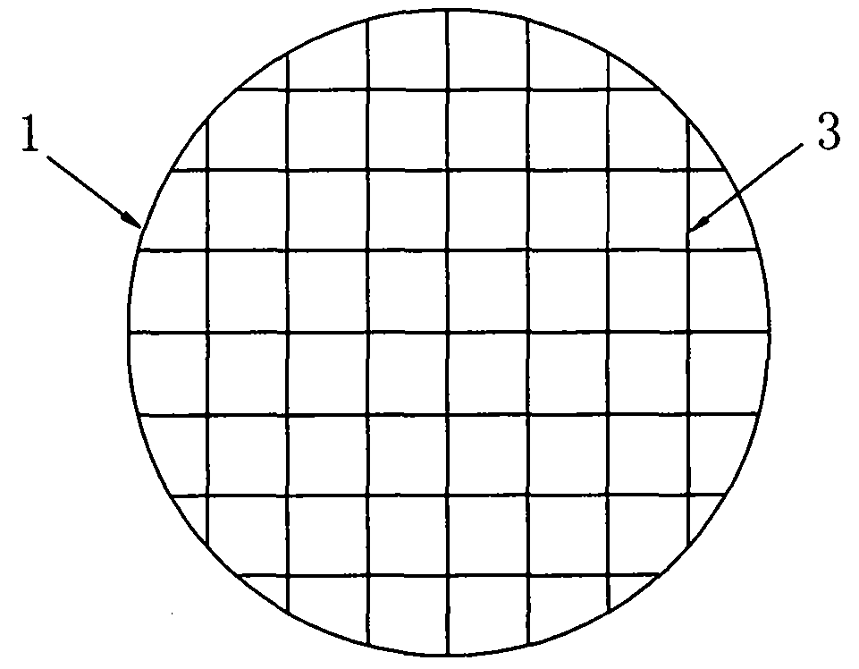
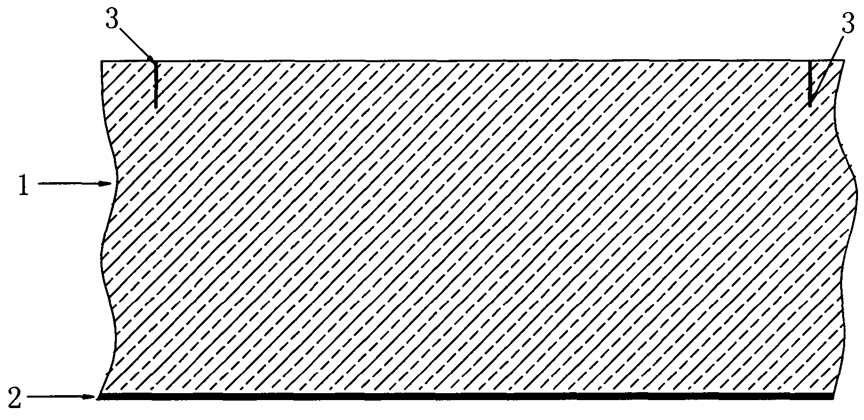
[0035] Example 1 please refer to Figures 1 to 2 , this embodiment involves the separation process of a GaN-based LED epitaxial chip with a sapphire crystal as a substrate, the epitaxial chip includes a 2-inch sapphire substrate 1 with a thickness of about 430 μm, and a GaN-based LED with a thickness of about 7 μm grown on the front side of the substrate. Epitaxial wafer layer 2.

[0036] The operation of separating the GaN-based LED epitaxial chip with the sapphire substrate is performed by a laser scribing process, which includes the following steps:

[0037] The LED epitaxial structure is cut and grown by a laser beam with a suitable wavelength (see "Laser Scribing Process of Sapphire Crystal Substrate for LEDs", "China Lighting Appliances", No. 3, 2010, and the invention patent with publication number CN100407461C, etc.) The backside of the sapphire substrate is formed with a number of trenches 3 with a depth of more than 43 μm, and the trenches correspond to predetermine...

Embodiment 2

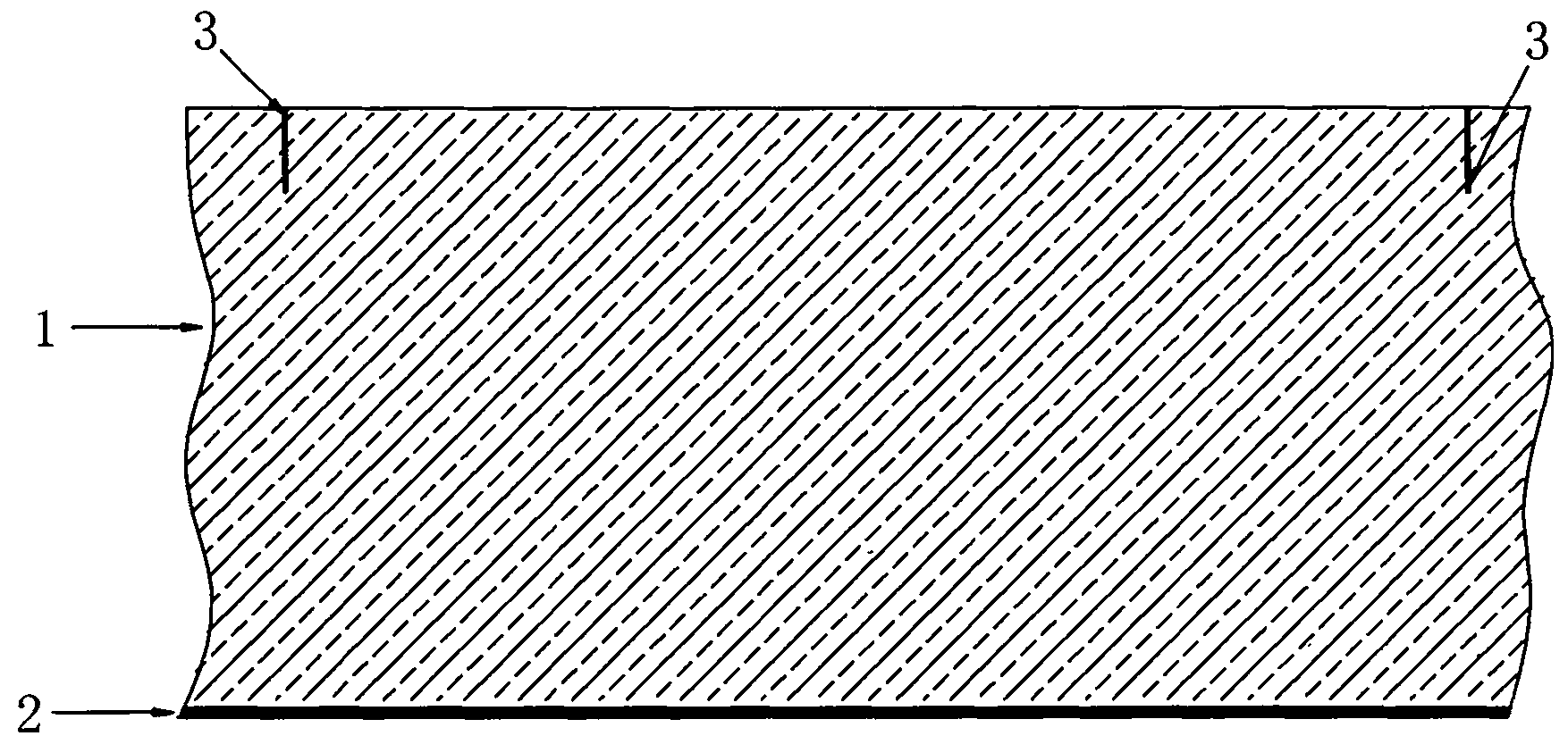
[0040] Embodiment 2 This embodiment involves the separation of a GaN-based LED epitaxial chip with a sapphire crystal as a substrate. The epitaxial chip includes a 4-inch sapphire substrate with a thickness of about 650 μm, and a sapphire substrate with a thickness of about 8 μm grown on the front surface of the substrate. GaN epitaxial wafer layers.

[0041] The operation of separating the GaN-based LED epitaxial chip with the sapphire substrate is performed by a laser scribing process, which includes the following steps:

[0042] The LED epitaxial structure is cut and grown by a laser beam with a suitable wavelength (see "Laser Scribing Process of Sapphire Crystal Substrate for LEDs", "China Lighting Appliances", No. 3, 2010, and the invention patent with publication number CN100407461C, etc.) The backside of the sapphire substrate is formed with several grooves with a depth of more than 65 μm, and the grooves correspond to the predetermined dividing positions between the ch...


PUM

PropertyMeasurementUnit
Thicknessaaaaaaaaaa
Thicknessaaaaaaaaaa
Horizontal sizeaaaaaaaaaa

Abstract

The invention discloses a separation method of an LED (light emitting diode) epitaxy chip, and the method comprises the following steps: forming a groove on the back of a hard substrate on which an LED epitaxy structure is reserved or grown in a photoetching manner, wherein the groove corresponds to a predetermined partition position between chip figures predetermined or formed at the frontage ofthe substrate; forming an epitaxy wafer on the epitaxy structure grown on the frontage of the substrate, and then partitioning the epitaxy wafer along the groove to form single LED epitaxy chips, or directly partitioning the epitaxy wafer along the groove to form single LED epitaxy chips, wherein the lateral dimension of each LED epitaxy chip is two or more than two times of the thickness of eachLED epitaxy chip, and the depth of the groove is more than one tenth of the thickness of each chip. By using the separation method of the LED epitaxy chip, the LED epitaxy chip is effectively simplified, especially the separation operation of a high-power LED epitaxy chip is simplified, the work efficiency and the yield of the LED chips are improved, and the production cost is reduced; and especially the LED chip based on a transparent substrate can be provided with a thicker transparent substrate utilized as a light-emitting window with high light-emitting efficiency, thus the method provided by the invention is especially suitable for the application of flip LED chip.

Description

technical field [0001] The invention relates to a method for preparing a semiconductor chip, in particular to a method for separating LED epitaxial chips based on a hard substrate. Background technique [0002] The new generation of semiconductor materials represented by GaN has great application potential in the fields of solid-state lighting, solid-state lasers, optical information storage, and ultraviolet detectors. [0003] At present, common GaN-based light-emitting elements mainly use wafers formed of materials such as sapphire and silicon carbide as substrates. The manufacturing process includes: growing on the substrate to form an epitaxial structure, and then cutting the substrate into individual LED chips. [0004] The traditional cutting method is to use a diamond knife as a cutting tool to cut the surface of the substrate first, and then perform the fracture process. However, substrates such as sapphire and silicon carbide have great hardness and strength, so cu...

Claims


Application Information

Patent Timeline
IPC IPC(8): H01L33/00H01L21/78B23K26/36B23K26/40B23K26/364B23K26/402
Inventor 梁秉文
Owner SUZHOU NAFANG TECH DEV
Why Eureka
Try Eureka