Method for manufacturing electrode for solar cell, substrate for solar cell manufactured by the same, and solar cell manufactured by the same

A technology of solar cells and manufacturing methods, applied in circuits, electrical components, photovoltaic power generation, etc., can solve the problems of low crystal defect density, low price, high price, etc., and achieve high productivity, improve efficiency, and reduce surface resistance.

Inactive Publication Date: 2011-10-12
SSCP CO LTD
View PDF2 Cites 10 Cited by
  • Summary
  • Abstract
  • Description
  • Claims
  • Application Information

AI Technical Summary

Problems solved by technology

The material in the single crystal form is a high-efficiency material with high purity and low crystal defect density, but the price is high; the material efficiency in the polycrystalline form is slightly lower than that of single crystal, but the price is relatively low and more popular

Method used


Image

  • Method for manufacturing electrode for solar cell, substrate for solar cell manufactured by the same, and solar cell manufactured by the same
  • Method for manufacturing electrode for solar cell, substrate for solar cell manufactured by the same, and solar cell manufactured by the same
  • Method for manufacturing electrode for solar cell, substrate for solar cell manufactured by the same, and solar cell manufactured by the same

Examples


Embodiment 1

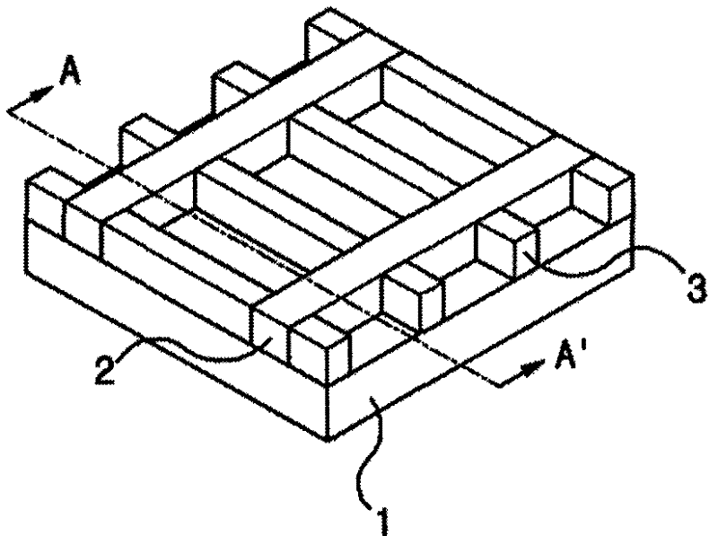
[0060]First, gravure offset printing was performed using a paste composition for offset printing (silver powder 68%, glass frit 17%, binder 10%, dilution solvent 3%, dispersant and others 2%). Use the scraper pressure and angle of the initial gravure roll to check the doctoring status, and adjust the off pressure and set by adjusting the off nip and set nip of the Blanket Roll. ) to adjust the pressure to the best state. After filling 20g of paste between the gravure roller and the doctor blade, doctoring is performed at a rotation speed of about 7 rpm. After scraping more than 3 times, let the paste off on the rubber of the guide roller at a speed of 7rpm, and then drive the guide roller to rotate one circle. During the rotation of the guide drum, the paste fully absorbed by the rubber is set at a speed of 7rpm. Conductive paste was printed once on a 5" wafer vacuum-fixed on a printing board as described above. After drying the printed substrate, it was fired in an infrared...

Embodiment 2

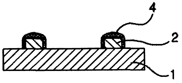
[0063] Except that the electrolytic copper plating and electroless silver plating are performed in the wet metal gold plating process of the embodiment 1, other steps are the same as the embodiment 1. At this time, the electrolytic copper plating is immersed in an electrolytic copper plating bath composed of 220g / l copper sulfate and 60ml / l sulfuric acid in terms of metal salts. A copper plate is used for the anode. / dm2, gold plating time of 10 minutes under the conditions of electrolytic copper plating film forming operation. Then, it was immersed in the silver plating bath used in the above-mentioned Example 1, and the principle of displacement gold plating method was carried out by the difference in the metal ionization tendency of the copper gold plating layer and the silver plating bath under the situation of no current flow for 5 minutes, and finally completed. The film-forming operation of the electroless silver gold-plated layer.


PUM


Abstract

The present invention provides a method for manufacturing an electrode for a solar cell, a substrate for the solar cell manufactured by the same, and a solar cell manufactured by the same. The present invention forms an electrode of a specific pattern through an offset printing system, and plates the electrode through a plating process to fill the metal-free region of a bus bar electrode with a plating metal and thus reduce the sheet resistance of the bus bar. The present invention obtains a finger electrode with a line width of 100 microns or less through the combination of an offset printing process and a wet metal plating process. Further, the present invention obtains an electrode with an aspect ratio of 0.2 to 0.6 to reduce light shield effects and improve efficiency of the solar cell.; The present invention eliminates the necessity of multi-layer offset printing, and thus to reduce use of expensive conductive paste which might otherwise increase in proportion to the number of times printing is performed.

Description

technical field [0001] The present invention relates to a method for manufacturing an electrode for a solar cell, a substrate for a solar cell manufactured by the method, and a solar cell. Background technique [0002] A solar cell is a semiconductor element that can convert solar energy into electrical energy. It has a p-n combination form, and its basic structure is the same as that of a diode. After light is incident on a solar cell, the incident light is absorbed by the solar cell and interacts with the substances that make up the semiconductors in the solar cell. As a result, electrons and holes are formed as minority carriers, and they move to both sides of the connected electrodes to generate electromotive force. [0003] Generally speaking, crystalline silicon solar cells (Crystalline Silicon Solar Cell) are mainly divided into two forms: single crystal (Single Crystal) and polycrystalline (Polycrystalline). The material in single crystal form is a high-efficiency ...

Claims


Application Information

Patent Timeline
Patent Type & Authority Applications(China)
IPC IPC(8): H01L31/042
CPCH01L31/022425Y02E10/50H01L31/04H01L31/0224H01L31/18
Inventor 李受珍康基伦郑贤珉李大成
Owner SSCP CO LTD
Why Eureka
Try Eureka