Manufacturing method of adjustable FP (filter pass) optical filter based on MEMS (micro electro mechanical system) process

An optical filter and filter technology, which is applied in the process, optics, and optical components for producing decorative surface effects, can solve the problems of complex manufacturing process, high manufacturing difficulty and high price of high-quality micro-concave mirrors. Achieve the effect of simple structure, fast tuning speed and easy mass production

Inactive Publication Date: 2011-10-26
SHANGHAI INST OF MICROSYSTEM & INFORMATION TECH CHINESE ACAD OF SCI
View PDF7 Cites 20 Cited by
  • Summary
  • Abstract
  • Description
  • Claims
  • Application Information

AI Technical Summary

Problems solved by technology

Axsun Corporation of the United States has developed an electrostatically driven MEMS FP tunable optical filter (patent number: 6373632B1), which adopts the design scheme of separating the FP interference cavity and the driver, and its FP interference cavity uses a flat-concave interference cavity to increase the size of the two-cavity mirror Parallelism tolerance, but the manufacturing process of high-quality micro-concave mirror compatible with MEMS process is complicated, difficult and expensive
Although Axsun has realized the market sales and spectral analysis applications of MEMS FP tunable optical filters, its manufacture is difficult and expensive

Method used


Image

  • Manufacturing method of adjustable FP (filter pass) optical filter based on MEMS (micro electro mechanical system) process
  • Manufacturing method of adjustable FP (filter pass) optical filter based on MEMS (micro electro mechanical system) process
  • Manufacturing method of adjustable FP (filter pass) optical filter based on MEMS (micro electro mechanical system) process

Examples


Embodiment Construction

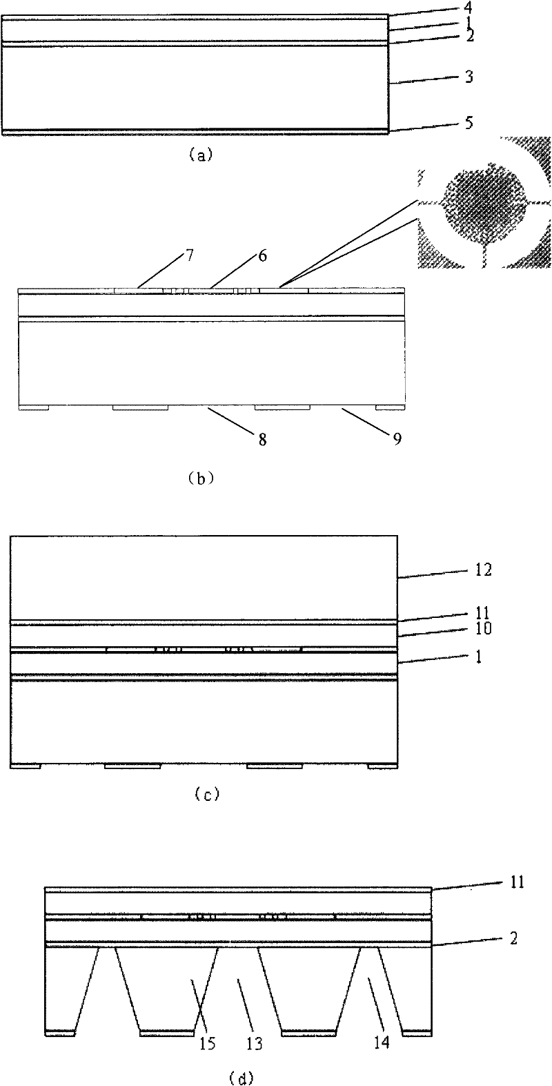
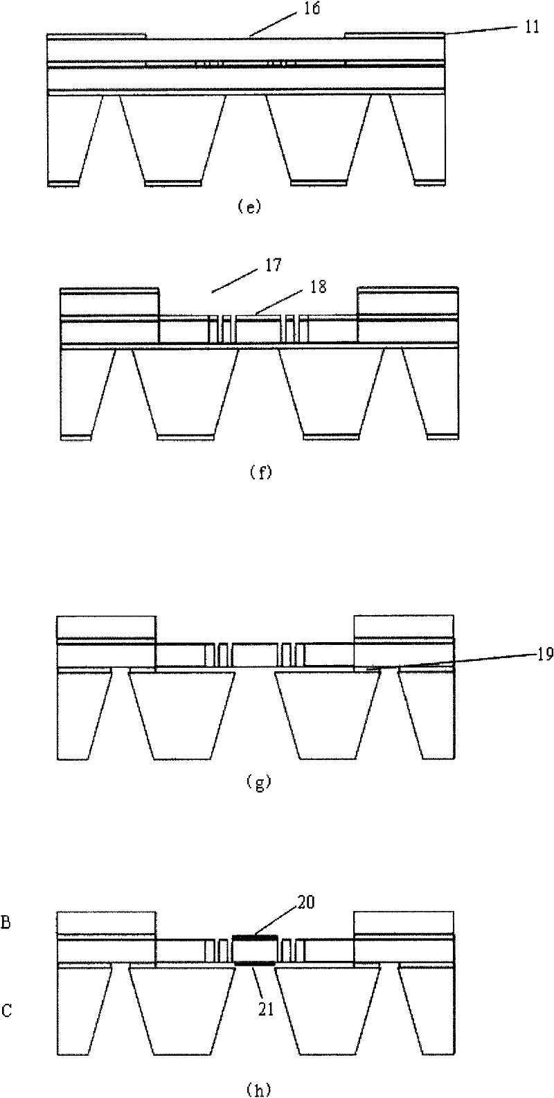
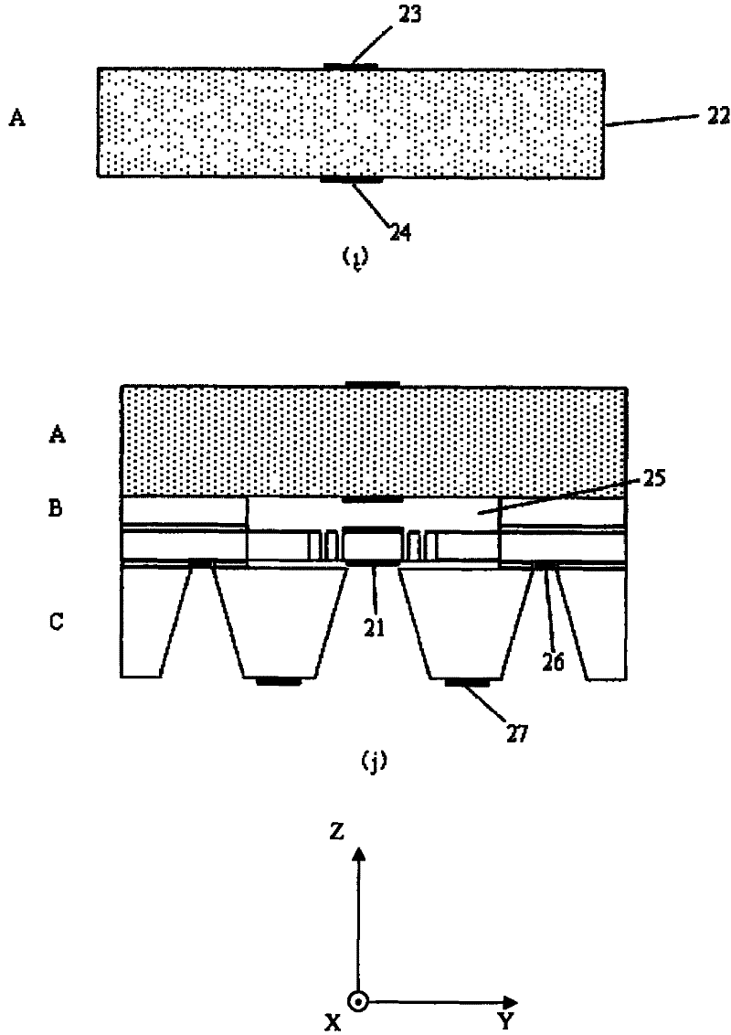
[0043] The various stages of manufacturing the FP cavity tunable filter provided by the present invention are further explained below with reference to the accompanying drawings. figure 2 An example of the FP tunable filter made. By referring to US patent 6373632B1, it is helpful to understand the manufacturing method and process of the present invention. The present invention is a practical and convenient method for manufacturing a MEMS flat-flat interference cavity FP tunable filter.

[0044] The detailed manufacturing process of the present invention will be described in detail below in conjunction with the accompanying drawings.

[0045] Step 1 realizes the manufacture of the cavity isolator B and the movable micromirror support structure C, and the process flow is as follows:

[0046] (a) Commercial low-resistance SOI used 1 The thickness of the silicon wafer is 30 μm for the top layer of silicon 1 , 2 μm for the thickness of the middle silicon dioxide layer 2 , and 38...


PUM

PropertyMeasurementUnit
thicknessaaaaaaaaaa
thicknessaaaaaaaaaa
thicknessaaaaaaaaaa

Abstract

The invention relates to a manufacturing method of an adjustable FP (filter pass) optical filter based on an MEMS (micro electro mechanical system) process, which is characterized in that the etching window of all graphs is manufactured by adopting the etching twice; the manufacturing of a middle FP air cavity and a movable reflector surface structure is finished by adopting the plasma silicon etching once; a movable silicon membrane reflector is manufactured by adopting the processes such as the silicon-silicon bonding, the plasma dry etching, the HF (hydrogen fluoride) acid etching and the silicon oxide layer releasing once; the high-reflection membrane and anti-reflection membrane of the two reflectors in the FP cavity are manufactured by adopting a method for selecting evaporation through a hard template; and a final FP cavity filter is formed by adopting the silicon-glass bonding once. In the manufacturing method provided by the invention, the process procedures are greatly simplified; the mirror finish and parallelism of the FP cavity are guaranteed; and the optical technical index and chip yield of the manufactured FP filter are improved. Compared with the existing like product manufacturing process, the manufacturing method provided by the invention has the advantages of good process compatibility and maneuverability, low driving voltage and good optical tuning repeatability and stability and can be widely applied to an optical communication WDM (wavelength division multiplex) system.

Description

technical field [0001] The invention relates to a MEMS manufacturing method of a Fabry-Perot cavity (Fabry-Perot, FP for short) tunable optical filter. It belongs to the field of micro-mechanics and adjustable laser production. Background technique [0002] Tunable optical filters have a wide range of applications in the fields of optical communication, fiber optic sensing, and fiber lasers. In optical communication, the tunable optical filter is used as the core optical splitting element in the optical performance detector (OPM), and the optical signal of a specific wavelength channel can be selected from the dense wavelength division multiplexing (DWDM) signal as the monitoring object as required. Realize the analysis and monitoring of optical signals in optical domain and electrical domain. In the optical add-drop multiplexer (OADM), the tunable optical filter has the multiplexing function of the reconfigurable optical signal add / drop, which can realize the flexible upl...

Claims


Application Information

Patent Timeline
Patent Type & Authority Applications(China)
IPC IPC(8): B81C1/00G02B26/00
Inventor 吴亚明翟雷应徐静李四华钟少龙
Owner SHANGHAI INST OF MICROSYSTEM & INFORMATION TECH CHINESE ACAD OF SCI
Why Eureka
Try Eureka