Electrode for realizing ohmic contact with n type ZnS quasi-one-dimensional nanometer material and preparation method thereof

A technology of nano-materials and ohmic contacts, applied in circuits, electrical components, semiconductor devices, etc., to achieve mature and reliable, simple preparation process, and easy-to-control effects

Inactive Publication Date: 2011-11-02
HEFEI UNIV OF TECH
View PDF5 Cites 6 Cited by
  • Summary
  • Abstract
  • Description
  • Claims
  • Application Information

AI Technical Summary

Problems solved by technology

ITO and AZO transparent electrodes have been widely used in electronic devices and optoelectronic devices, such as displays, solar cells, etc., due to their high transmittance, electrical conductivity, relatively com...

Method used


Image

  • Electrode for realizing ohmic contact with n type ZnS quasi-one-dimensional nanometer material and preparation method thereof
  • Electrode for realizing ohmic contact with n type ZnS quasi-one-dimensional nanometer material and preparation method thereof
  • Electrode for realizing ohmic contact with n type ZnS quasi-one-dimensional nanometer material and preparation method thereof

Examples


Embodiment 1

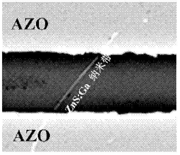
[0027] The doping concentration synthesized by chemical vapor deposition method is 1.0×10 16 cm -3 Ga-doped ZnS nanoribbons uniformly dispersed in SiO with a thickness of 300 nm 2 On the p-type heavily doped Si wafer, the bottom gate of the device is on the p-type heavily doped Si wafer, the photoresist is uniformly spin-coated, and the two-electrode electrode pattern is photo-etched. figure 1 SEM image of the device.

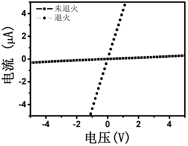
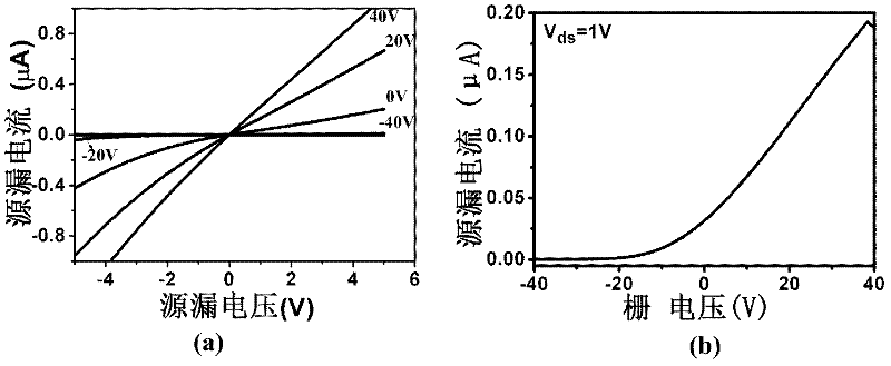
[0028] Using the pulsed laser deposition method, the condition is that the laser energy is 40mJ, the laser wavelength is 248nm, the pulse frequency is 20Hz, and the vacuum degree is 1×10 -5 Pa, deposit a 60nm thick AZO film on the photoetched electrode pattern. In order to further reduce the contact resistance between the AZO electrode and Ga-doped ZnS nanoribbons, the AZO electrode was vacuumed at 10 -4 Under Pa annealing, the annealing temperature is 100° C., and the time is 5 minutes. KEITHLEY 4200 semiconductor characteristic testing system was used to...

Embodiment 2

[0030] The doping concentration synthesized by chemical vapor deposition method is 2.0×10 17 cm -3 Cl-doped ZnS nanowires were uniformly dispersed in SiO with a thickness of 300 nm 2 On the p-type heavily doped Si wafer, the p-type heavily doped Si wafer is the bottom gate of the device, and the photoresist is evenly spin-coated, and the two-electrode electrode pattern is photoetched.

[0031] Using the pulsed laser deposition method, the condition is that the laser energy is 400mJ, the laser wavelength is 248nm, the pulse frequency is 1Hz, and the vacuum degree is 1×10 -2 Pa, deposit a 60nm thick AZO film on the photoetched electrode pattern. In order to further reduce the contact resistance between the AZO electrode and the Cl-doped ZnS nanowires, the AZO electrode was vacuumed at 10 -2 Under Pa annealing, the annealing temperature is 600° C., and the time is 30 minutes. The electrical transport properties of Cl-doped ZnS nanowires were tested by KEITHLEY 4200 semiconduc...

Embodiment 3

[0033] The doping concentration synthesized by chemical vapor deposition method is 6.0×10 15 cm -3 Al-doped ZnS nanoribbons uniformly dispersed in SiO with a thickness of 300 nm 2 On the p-type heavily doped Si wafer, the p-type heavily doped Si wafer is the bottom gate of the device, and the photoresist is evenly spin-coated, and the two-electrode electrode pattern is photoetched.

[0034]Using the magnetron sputtering method, the condition is that the air pressure is 1Pa, the sputtering power is 40W, and the Ar gas flow rate is 10sccm, and a 60nm thick AZO film is deposited on the photoetched electrode pattern. In order to further reduce the contact resistance between the AZO electrode and the Al-doped ZnS nanobelt, the AZO electrode was 2 The annealing is carried out under atmosphere protection, the annealing temperature is 300° C., and the annealing time is 20 minutes. The KEITHLEY 4200 semiconductor characteristic testing system was used to test the electrical transpor...


PUM


Abstract

The invention discloses an electrode for realizing an ohmic contact with an n type ZnS quasi-one-dimensional nanometer material and a preparation method thereof. The electrode provided in the invention is characterized in that the electrode is AZO or ITO transparent electrodes and is directly formed on the n type ZnS quasi-one-dimensional nanometer material. The electrode is prepared by a magnetron sputtering method or a pulsed laser deposition method and the prepared electrode is processed by a post-annealing treatment, so that the ohmic contact between the electrode and the ZnS quasi-one-dimensional nanometer material can be further improved. According to the invention, the problem of the direct ohmic contact between the electrode and the n type ZnS quasi-one-dimensional nanometer material can be solved. The electrode provided in the invention can be used for preparation and research of relevant devices of the n type ZnS quasi-one-dimensional nanometer material. Moreover, the preparation method of the electrode is simple, reliable and is easy to operate.

Description

technical field [0001] The invention belongs to the technical field of semiconductor devices, and in particular relates to an electrode in ohmic contact with an n-type ZnS material and a preparation method thereof. Background technique [0002] One-dimensional nanomaterials have become a research hotspot in nanotechnology due to their novel physical, chemical and biological properties and their potential applications in nanodevices. The large amount, low cost, simple and effective synthesis and assembly of one-dimensional nanomaterials are of special significance not only from the perspective of basic research, but also from the perspective of performance and application. Semiconductor nanomaterials have potential applications in optics, electricity, magnetism, and nanoelectronics, and are one of the research hotspots in nanomaterials science in recent years. Zinc sulfide ZnS is one of the most important II-VI group direct bandgap semiconductors. The ZnS band gap is 3.7eV. ...

Claims


Application Information

Patent Timeline
IPC IPC(8): H01L29/45H01L31/0224H01L21/28
Inventor 揭建胜于永强蒋阳罗林保朱志峰
Owner HEFEI UNIV OF TECH
Why Eureka
Try Eureka