Low-gate charge low-on resistance deep trench power metal oxide semiconductor field effect transistor (MOSFET) device and manufacturing method

A low on-resistance, deep trench technology, applied in semiconductor/solid-state device manufacturing, semiconductor devices, electrical components, etc., can solve the problems of reducing gate-drain capacitance Cgd, reducing gate charge, reducing characteristic on-resistance, etc., to achieve Reduced gate-to-drain parasitic capacitance Cgd, reduced characteristic on-resistance, and reduced characteristic on-resistance

Active Publication Date: 2012-11-07
WUXI NCE POWER
View PDF1 Cites 0 Cited by
  • Summary
  • Abstract
  • Description
  • Claims
  • Application Information

AI Technical Summary

Problems solved by technology

However, when the unit cell density increases, the corresponding gate charge will also increase, and it is difficult to reduce both the on-resistance and the gate charge at the same time; the second is to increase the doping concentration of the epitaxial wafer and reduce the thickness of the epitaxial layer, but this The method will reduce the source-drain breakdown voltage, so relying solely on reducing the doping concentration / reducing the thickness of the epitaxial layer is limited by the size requirement of the breakdown voltage
There are many ways to reduce the gate charge. For example, Hua Hong NEC Electronics’ patent application in China (publication number CN1877856A) proposed thick bottom oxide technology (Thick bottom oxide) to reduce the gate-to-drain capacitance Cgd, thereby reducing the gate charge. For the purpose of Qg, this technology reduces Qg by about 30%, but it still cannot meet the increasingly high frequency applications, and cannot significantly reduce the characteristic on-resistance at the same time

Method used


Image

  • Low-gate charge low-on resistance deep trench power metal oxide semiconductor field effect transistor (MOSFET) device and manufacturing method
  • Low-gate charge low-on resistance deep trench power metal oxide semiconductor field effect transistor (MOSFET) device and manufacturing method
  • Low-gate charge low-on resistance deep trench power metal oxide semiconductor field effect transistor (MOSFET) device and manufacturing method

Examples


Embodiment 1

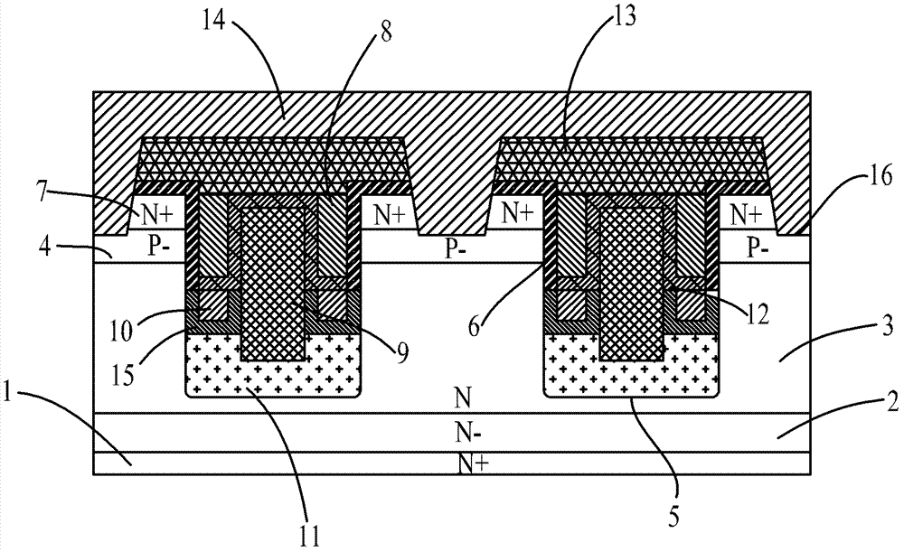
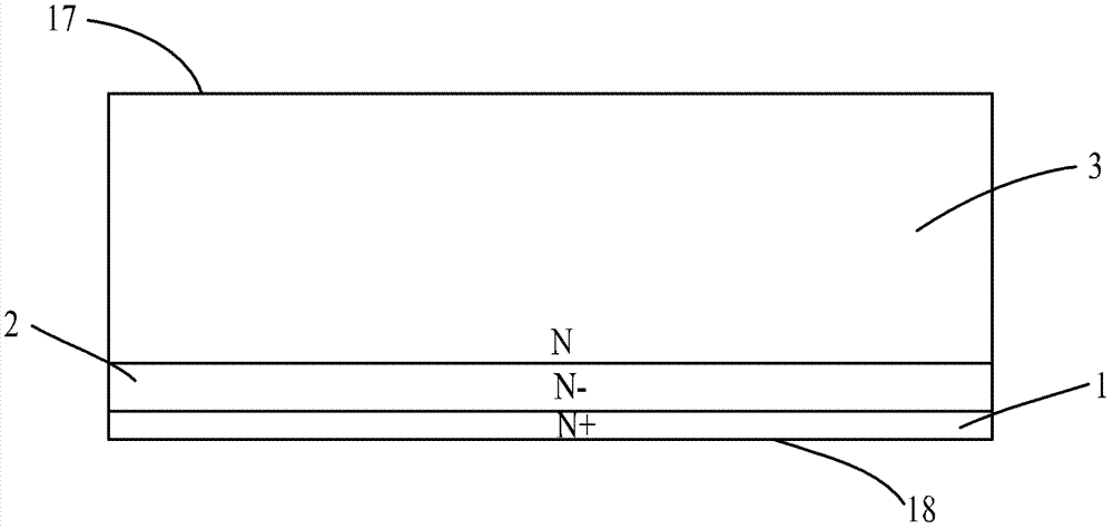
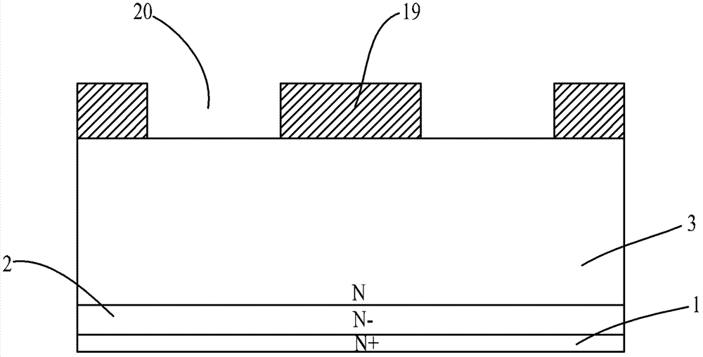
[0068] Such as Figure 1~Figure 18 As shown: taking an N-type power MOSFET device as an example, the present invention includes an N-type drain region 1, an N-type first epitaxial layer 2, an N-type second epitaxial layer 3, a P well layer 4, a cell trench 5, an insulating Gate oxide layer 6, N+ source region 7, gate conductive polysilicon 8, first shielded gate conductive polysilicon 9, second shielded gate conductive polysilicon 10, shielded gate oxide layer 11, insulating dielectric layer 12 between conductive polysilicon, insulating dielectric layer 13. Metal wiring 14, first isolation oxide layer 15, contact hole 16, first main surface 17, second main surface 18, hard mask layer 19, hard mask window 20, second oxide layer 21, first Polysilicon deposition tank 22, first conductive polysilicon layer 23, third oxide layer 24, second polysilicon deposition tank 25, fourth oxide layer 26, fifth oxide layer 27 and third polysilicon deposition Slot 28.

[0069] Such as figure...

Embodiment 2

[0108] like Figure 19~Figure 36 As shown: taking an N-type power MOSFET device as an example, the present invention includes an N-type drain region 1, an N-type first epitaxial layer 2, an N-type second epitaxial layer 3, a P well layer 4, a cell trench 5, an insulating Gate oxide layer 6, N+ source region 7, gate conductive polysilicon 8, second shielded gate conductive polysilicon 10, shielded gate oxide layer 11, insulating dielectric layer 12 between conductive polysilicon, insulating dielectric layer 13, metal wiring 14, the second An isolation oxide layer 15, a contact hole 16, a first main surface 17, a second main surface 18, a second oxide layer 21, a first polysilicon deposition groove 22, a first conductive polysilicon layer 23, and a third oxide layer 24 , the second polysilicon deposition groove 25, the fourth oxide layer 26, the fifth oxide layer 27, the third polysilicon deposition groove 28, the third shielded gate conductive polysilicon 29, the fourth shielde...


PUM


Abstract

The invention relates to a low-gate charge low-on resistance deep trench power metal oxide semiconductor field effect transistor (MOSFET) device and a manufacturing method. Shield grid conducting polycrystalline silicon bodies are arranged in cellular trenches of the device. The two sides of the shield grid conducting polycrystalline silicon body are provided with gate conducting polycrystalline silicon. An insulating gate oxide layer is arranged between the gate conducting polycrystalline silicon and the upper sidewall of the cellular trench. Second shield grid conducting polycrystalline silicon is arranged below the gate conducting polycrystalline silicon. A shield grid oxide layer covers the lower part of the shield grid conducting polycrystalline silicon. A trench opening of the cellular trench is covered by an insulating dielectric layer. The two sides of the cellular trench are provided with a contact hole respectively. Metal connecting wires are deposited on the insulating dielectric layer, are in ohmic contact with a first-conduction type source region and a second-conduction type well layer and realize gate conducting polycrystalline silicon electrical connection, shield grid conducting polycrystalline silicon body electrical connection and second shield grid conducting polycrystalline silicon electrical connection. The device is low in on resistance, gate-drain charge (Qgd), switching loss and cost and high in switching speed; and a process is simple.

Description

technical field [0001] The invention relates to a power MOSFET device and a manufacturing method thereof, in particular to a low gate charge and low on-resistance deep trench power MOSFET device and a manufacturing method thereof, belonging to the technical field of semiconductor devices. Background technique [0002] Trench power MOS devices have the characteristics of high integration, low on-resistance, fast switching speed, and low switching loss, and are widely used in various power management and switching conversions. With the development of industry and global warming, the climate environment is getting worse and worse. Countries have begun to pay more and more attention to energy saving, carbon reduction and sustainable development. Therefore, the requirements for power consumption and conversion efficiency of power MOS devices are getting higher and higher. The conduction loss is mainly composed of conduction loss and switching loss. The conduction loss is mainly a...

Claims


Application Information

Patent Timeline
Patent Type & Authority Patents(China)
IPC IPC(8): H01L29/78H01L29/40H01L29/423H01L21/336
Inventor 朱袁正秦旭光丁磊叶鹏
Owner WUXI NCE POWER
Why Eureka
Try Eureka