Preparation method of hollow-structured micro-array electrode

A micro-array electrode, micro-electrode technology, applied in the directions of micro-structure technology, micro-structure device, manufacturing micro-structure device, etc., can solve problems such as difficulty, difficulty in realizing micro-electrode array heterogeneity, and inability to prepare micro-electrode array, etc. Achieve the effect of low cost, rich structural forms and diverse shapes

Inactive Publication Date: 2012-01-18
SHANGHAI JIAO TONG UNIV
View PDF8 Cites 16 Cited by
  • Summary
  • Abstract
  • Description
  • Claims
  • Application Information

AI Technical Summary

Problems solved by technology

However, due to the use of mechanical cutting and grinding, there will be metamorphic layers and microcracks on the processed surface, and it is difficult to realize the anisotropy of the microelectrode array. Secondly, it is difficult to mechanically process micron-scale anisotropic electrodes, and it cannot be prepared. microelectrode array

Method used


Image

  • Preparation method of hollow-structured micro-array electrode
  • Preparation method of hollow-structured micro-array electrode
  • Preparation method of hollow-structured micro-array electrode

Examples


Embodiment 1

[0035] 1) Make mask plate;

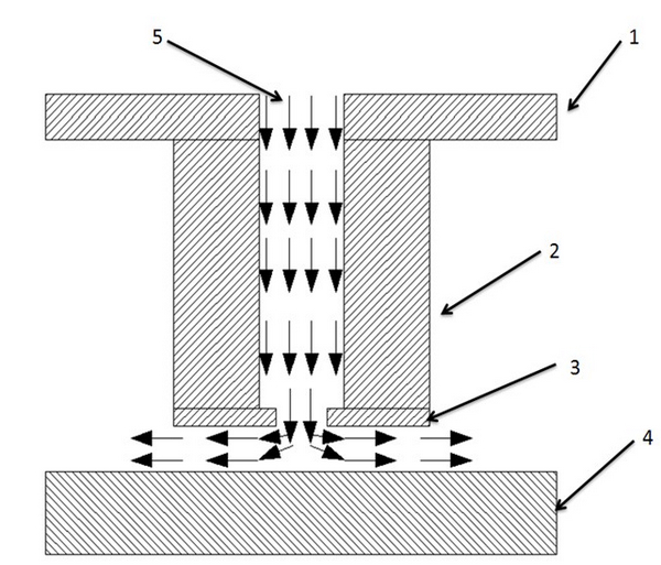
[0036] The production of the electrode is divided into three layers. The mask plate of the first layer can be a film plate, and the mask plate of the second and third layers can be made of a high-precision chromium plate. The mask on the second and third layers of the mask plate is rectangular. ;

[0037] 2) On a 3-inch glass slide, 1um Ti was sputtered at 65°C in a mass fraction of 2% NaOH and 1% H 2 O 2 Oxidation in the mixed solution for 3min to form uniform and dense black TiO 2 To ensure good adhesion between the substrate and the photoresist, dry it at 180°C for 4 hours, then throw the SU-8-50 negative photoresist 300um, and then perform pre-baking, exposure for 180s, and middle-baking in sequence , Development, according to the shape of the electrode designed by the mask plate, the patterning of the support layer of the micro-electrode array bottom plate is realized;

[0038] 3) After removing the residual negative gel...

Embodiment 2

[0046] 1) Make a mask; the production of the electrode is divided into three layers, the mask of the first layer can be a film plate, the mask of the second and third layers is a chrome plate with high precision, the second and third layers of masks The mask on the stencil is a triangle;

[0047] 2) On a 4 inch piece of glass, sputter 800 Ti, then repeat step 2) of Example 1 to realize the patterning of the support layer of the microelectrode array bottom plate;

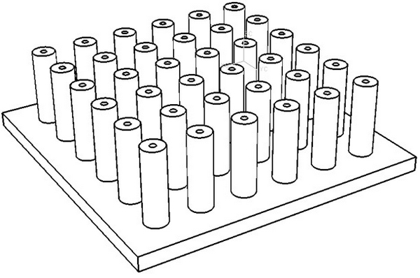
[0048] 3) After removing the residual negative glue on the sheet with a glue remover, perform activation cleaning, and deposit Ni by electrodeposition, and the plating solution is the same as step 3) of Example 1. At a temperature of 45°C, a pH of 4, and a current density of 15mA / cm2, electroplating for 16 hours to obtain a bright, uniform microarray electrode base plate with a thickness of about 300um;

[0049] 4) After flattening the nickel microarray electrode base plate obtained by electroplating wit...

Embodiment 3

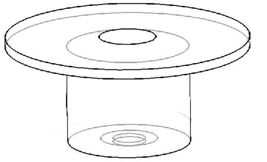
[0056] 1) Make a mask; the production of the electrode is divided into three layers, the mask of the first layer can be a film plate, the mask of the second and third layers is a chrome plate with high precision, the second and third layers of masks The mask on the stencil is circular;

[0057] 2) On a 6-inch piece of glass, sputter 900 Ti, then repeat step 2) of Example 1 to realize the patterning of the support layer of the microelectrode array bottom plate;

[0058] 3) After removing the residual negative glue on the sheet with a glue remover, perform activation cleaning, and deposit Ni by electrodeposition, and the plating solution is the same as step 3) of Example 1. At a temperature of 45°C, a pH of 4, and a current density of 20mA / cm2, electroplating for 12 hours to obtain a bright, uniform microarray electrode base plate with a thickness of about 300um;

[0059] 4) Planarize the nickel microarray electrode bottom plate obtained by electroplating with plana...


PUM


Abstract

The invention belongs to the technical field of micromachining, and discloses a preparation method of a hollow-structured micro-array electrode. The method comprises steps that: (1) a mask plate is prepared; (2) a metal Ti thin layer is sputtered onto a glass sheet; an oxidation treatment is carried out; an SU8 photoresist spinning treatment, a pre-baking process, and the like are carried out, such that the visualization of an electrode photoresist structure is realized; (3) with an electro-deposition technology, a microelectrode supporting pedestal is formed; (4) SU8 photoresist spinning photoetching is carried out again; (5) with the electro-deposition technology, a hollow cylinder is formed, wherein the hollow cylinder is an electrode; (6) a Gr / Cu conductive layer is formed through sputtering; (7) positive photoresist spinning photoetching is carried out; (8) electro-deposition is carried out until a third layer of the microelectrode is reached; and (9) the electrode is smoothed, and photoresist is removed. The method can be used for producing hollow-structured microelectrodes of any shapes, wherein the microelectrodes are used in high-precision fine electrochemical machining appliances. Also, the method can be applied in mass productions.

Description

technical field [0001] The invention relates to a method for preparing a microarray electrode with a hollow structure, which belongs to the technical field of microfabrication. Background technique [0002] With the development of emerging micro-electromechanical systems (MEMS), there is an urgent need for high-precision micro-machines, which is accompanied by the continuous increase of a large number of small-sized structures and high-precision parts of various shapes. As a typical microstructure, the micro-hole array has been widely used in MEMS, aerospace, precision instruments, chemical fiber and other fields, such as high-speed printer nozzle plate, optical fiber connector, chemical fiber spinneret, etc. Microfabrication is the basis and key technology for the realization of microstructures. Electrolytic machining is not limited by the mechanical properties of materials, the processing speed is fast, and it can achieve better surface roughness. There is no internal str...

Claims


Application Information

Patent Timeline
Patent Type & Authority Applications(China)
IPC IPC(8): B81C1/00
Inventor 汪红吴静丁桂甫赵小林
Owner SHANGHAI JIAO TONG UNIV
Why Eureka
Try Eureka