High-efficiency crystalline silicon cell with next-generation structure and manufacturing method for high-efficiency crystalline silicon cell

A technology of crystalline silicon cells and production methods, applied in circuits, photovoltaic power generation, electrical components, etc., can solve problems such as restricting the improvement of cell efficiency, and achieve the effects of improving efficiency, reducing resistance, and getting rid of dependence

Inactive Publication Date: 2012-03-21
CHINA UNITED CLEANING TECH BEIJING
View PDF7 Cites 16 Cited by
  • Summary
  • Abstract
  • Description
  • Claims
  • Application Information

AI Technical Summary

Problems solved by technology

[0004] However, the current MWT technology still has not got rid of the dependence on expensive screen printing silver paste, and the various resistanc

Method used


Image

  • High-efficiency crystalline silicon cell with next-generation structure and manufacturing method for high-efficiency crystalline silicon cell
  • High-efficiency crystalline silicon cell with next-generation structure and manufacturing method for high-efficiency crystalline silicon cell
  • High-efficiency crystalline silicon cell with next-generation structure and manufacturing method for high-efficiency crystalline silicon cell

Examples


Embodiment 1

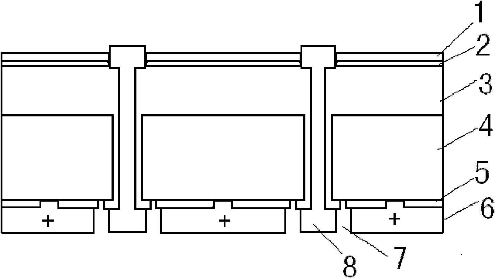
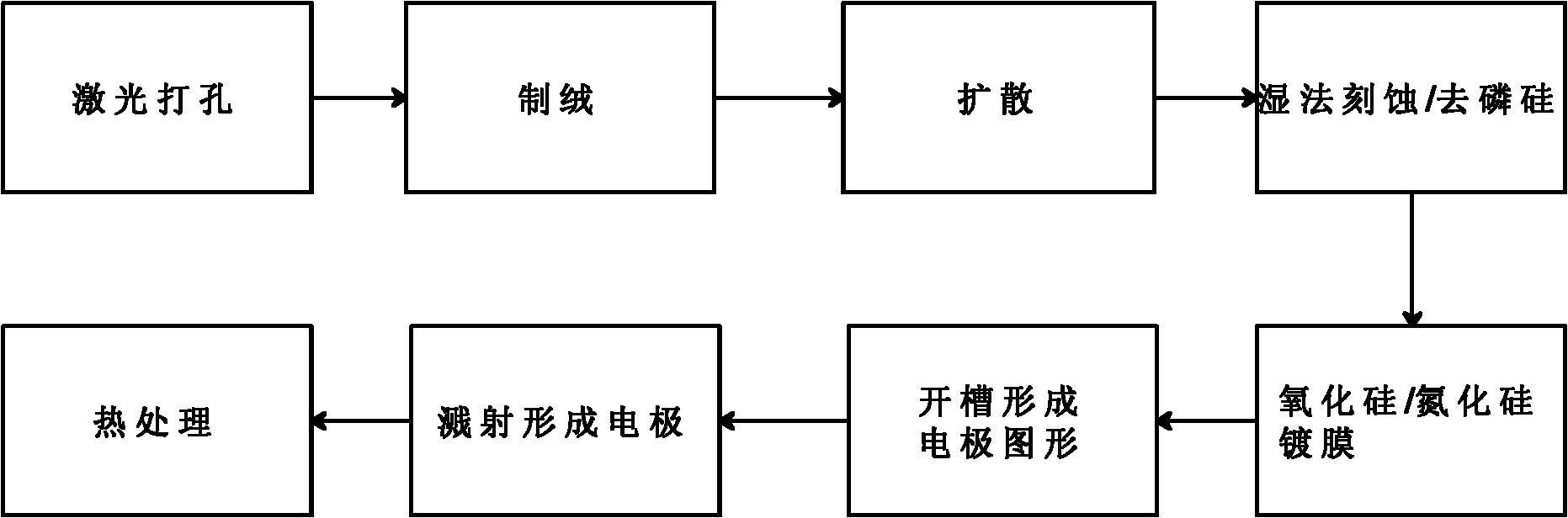
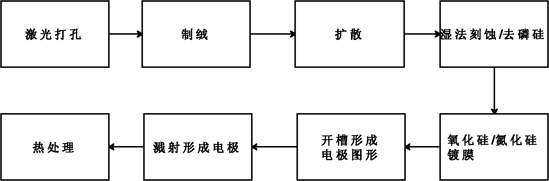
[0031] Embodiment 1: as figure 1 , 2 shown;

[0032] A method for manufacturing high-efficiency crystalline silicon solar cells, adding silicon oxide and aluminum oxide passivation steps, MWT technology steps, and new grid line forming steps on the basis of conventional processes; including the following steps;

[0033] In the laser drilling step, a laser is used to form 4*4 round holes with a diameter of about 300 microns on the surface of the 156mm*156mm polysilicon wafer, penetrating the silicon wafer;

[0034] Texturing step, using HNO3 / HF / H2O system (nitric acid / hydrofluoric acid / water system), nitric acid is electronically pure, with a mass concentration of about 69%; hydrofluoric acid is electronically pure, with a mass concentration of about 49%; water is deionized Water, the resistance value is about 18 megohm cm; the volume ratio of the three is about 6.5:1:3; the temperature is 8-11°C. Clean the surface of the silicon wafer and form a suede surface;

[0035] In ...

Embodiment 2

[0041] Embodiment 2: as figure 1 , 2 shown;

[0042] A method for manufacturing high-efficiency crystalline silicon solar cells, adding silicon oxide and aluminum oxide passivation steps, MWT technology steps, and new grid line forming steps on the basis of conventional processes; including the following steps;

[0043] In the laser drilling step, a laser is used to form 4*4 round holes with a diameter of about 250 microns on the surface of the 156mm*156mm single / polycrystalline silicon wafer, which penetrate the silicon wafer;

[0044] Or: laser drilling step, using a laser to form 3*3 9 round holes with a diameter of about 250 microns on the surface of the 125mm*125mm single / polycrystalline silicon wafer, penetrating the silicon wafer;

[0045] In the texturing step, polycrystalline use HNO3 / HF / H2O (nitric acid / hydrofluoric acid / water) system to clean the surface of the silicon wafer and form a textured surface; single crystal uses NaOH / IPA / H2O (sodium hydroxide / isopropano...


PUM

PropertyMeasurementUnit
Resistanceaaaaaaaaaa

Abstract

The invention discloses a high-efficiency crystalline silicon cell with a next-generation structure and a manufacturing method for the high-efficiency crystalline silicon cell, and belongs to the field of crystalline silicon solar cells. The method comprises: a silicon oxide passivation step of forming a layer of silicon oxide film on the phosphorus-doped surface of a P-type silicon chip; an aluminum oxide passivation step of forming a layer of aluminum oxide film on the undoped surface of the P-type silicon chip; a metal wrap through (MWT) technology step of leading the anode of the cell to a back surface by adopting laser boring; and a new grid line formation step of adopting electroplating and sputtering. By the cell and the method, MWT is effectively combined, and the passivation of double film layers on a front surface and the passivation of aluminum oxide on the back surface are realized; due to the adoption of novel cell formation schemes such as electroplating, sputtering and the like, dependence on screen printing silver paste is overcome, and simultaneously resistance produced by electrodes is decreased; and the efficiency of a P-type monocrystalline cell can be improvedto over 20 percent, and the efficiency of a P-type polycrystalline cell can be improved to over 18 percent.

Description

technical field [0001] The invention relates to a high-efficiency crystalline silicon cell with a next-generation structure and a manufacturing method, belonging to the field of crystalline silicon solar cells. Background technique [0002] At present, due to factors such as optical loss, electron-hole recombination, and various resistance losses related to electrodes, there is still a lot of room for improvement in efficiency of crystalline silicon solar cells. [0003] In order to improve the photoelectric conversion efficiency of the cell, it is necessary to absorb and convert more photons. Reducing surface reflection and increasing light-receiving area are important ways to increase photon absorption. Reducing surface reflection is usually achieved by surface texture and anti-reflection coating. However, the reflection of light by the surface electrodes still restricts the absorption of light by the cell sheet. Thinning surface electrodes and adopting new electrode st...

Claims


Application Information

Patent Timeline
IPC IPC(8): H01L31/0352H01L31/04H01L31/068
CPCY02E10/50Y02E10/547
Inventor 孙良欣胡盛华
Owner CHINA UNITED CLEANING TECH BEIJING
Why Eureka
Try Eureka