Method for electrochemical preparation of cadmium telluride semiconductor film under alkaline water phase condition

An alkaline condition, electrochemical technology, applied in the direction of chemical instruments and methods, semiconductor devices, circuits, etc., to achieve the effect of reducing corrosion, solving needle-like pores, and reducing interface state density

Active Publication Date: 2012-03-28
UNIV OF JINAN
View PDF5 Cites 12 Cited by
  • Summary
  • Abstract
  • Description
  • Claims
  • Application Information

AI Technical Summary

Problems solved by technology

[0004] In order to solve the above problems that electrodeposition can only be deposited at a low cathode potential under alkaline conditions, and the shrinkage rate of the obtained film is large, resulting in a large number of voids and poor uniformity. The invention provides a method for electrochemically preparing cadmium telluride semiconductor thin films by directly preparing crystalline CdTe thin films by electrochemical deposition under aqueous alkaline conditions, reducing high-temperature crystallization shrinkage and improving density.

Method used


Image

  • Method for electrochemical preparation of cadmium telluride semiconductor film under alkaline water phase condition
  • Method for electrochemical preparation of cadmium telluride semiconductor film under alkaline water phase condition
  • Method for electrochemical preparation of cadmium telluride semiconductor film under alkaline water phase condition

Examples


Embodiment 1

[0035] (1) Preparation of CdTe Alkaline Precursor Deposition Solution

[0036] According to 0.005M tellurium dioxide (TeO 2 ), 0.005M cadmium sulfate (3CdSO 4 ·8H 2 O) and the amount of complexing agent nitrilotriacetic acid (NTA) of 0.005M. Put the three kinds of raw materials into a large beaker filled with 50mL deionized water. Adjust the pH to 7.8 and stir well to make the TeO 2 , cadmium sulfate and NTA are all dissolved and set aside;

[0037] (2) Electrochemical deposition of CdTe thin films

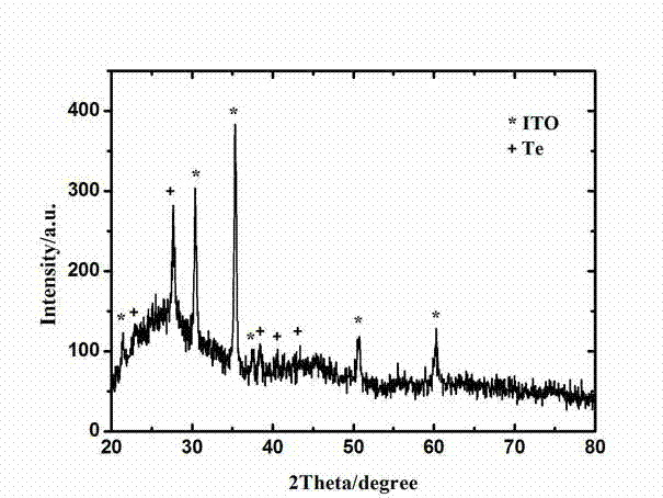
[0038] Put the cleaned ITO conductive glass in the alkaline precursor deposition solution prepared in step (1), and deposit it at 20°C for 10 minutes at the cathode potential of the -1.0V vs. HgO / KOH reference electrode, and take out the CdTe film. Rinse with deionized water and dry at 100 °C. XRD test results such as Figure 1a , containing a small amount of elemental Te;

[0039] (3) Post-processing of CdTe thin film

[0040]Transfer the CdTe film prepared in step (2) ...

Embodiment 2

[0042] (1) Preparation of CdTe Alkaline Precursor Deposition Solution

[0043] According to 0.001 M tellurium dioxide (TeO 2 ), 0.005M cadmium sulfate (3CdSO 4 ·8H 2 O) and 0.01 M of nitrilotriacetic acid (NTA) put the three raw materials into a large beaker filled with 50 mL of deionized water, the molar ratio of cadmium salt and complexing agent is 1:2, and the pH of the solution is adjusted to 8.4 , fully stirred to dissolve all, set aside;

[0044] (2) Electrochemical deposition of CdTe thin films

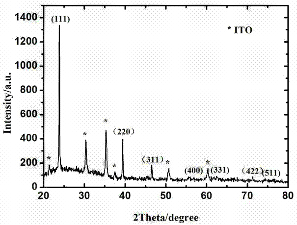
[0045] Put the cleaned ITO conductive glass in the CdTe alkaline precursor deposition solution prepared in step (1), and deposit it at 30°C for 20 minutes at the cathode potential of -1.1V vs. HgO / KOH reference electrode, and take out the CdTe film , washed with deionized water, and dried at 100 °C. The crystal structure of the obtained film is as Figure 4 As shown, there is only the diffraction peak of ITO, but no obvious CdTe peak;

[0046] (3) Post-processing of CdTe...

Embodiment 3

[0049] (1) Preparation of CdTe Alkaline Precursor Deposition Solution

[0050] According to 0.005M tellurium dioxide (TeO 2 ), 0.01M cadmium acetate (C 4 h 6 CdO 4 2H 2 O) and the amount of nitrilotriacetic acid (NTA) of 0.025M put the three raw materials into a large beaker filled with 50mL deionized water, the molar ratio of cadmium salt and complexing agent is 1:2.5, and the pH is adjusted to 8.7 , fully stirred to dissolve all, set aside;

[0051] (2) Electrochemical deposition of CdTe thin films

[0052] Put the cleaned ITO conductive glass in the CdTe alkaline precursor deposition solution prepared in step (1), and deposit it at 35°C for 30 minutes at the cathode potential of the -1.2V vs. HgO / KOH reference electrode, and take out the CdTe film , washed with deionized water, and dried at 100 °C. crystal structure and Figure 4 resemblance;

[0053] (3) Post-processing of CdTe thin film

[0054] Transfer the CdTe film prepared in step (2) to a rapid annealing fu...


PUM


Abstract

The invention relates to the technical field of cadmium telluride semiconductor film preparation, and relates to a method for electrochemical preparation of a cadmium telluride semiconductor film under an alkaline water phase condition; a three-electrode electrochemical deposition system is adopted; a CdTe film is electrochemically deposited on a deposition substrate from an alkaline precursor deposition solution at a temperature of 20 DEG C-80 DEG C and a cathodic deposition potential of from -1.0 V to -2.0 V; and the crystallization quality of the film is improved by performing annealing treatment of the deposited CdTe film. A high cathodic potential is adopted to avoid the problem of cracking caused by film polycondensation of amorphous CdTe during later thermal crystallisation treatment, wherein the amorphous CdTe is formed at a low cathodic potential; a weak alkaline solution is adopted to reduce the corrosion of the deposition substrate by the electrolyte solution; the H+ ion concentration of the weak alkaline solution is low, and thus less H2 gas is generated during the electrodeposition process, which avoids the problem of acicular pores caused by hydrogen generation during the deposition process, and greatly improves the film density and photoelectric properties.

Description

technical field [0001] The invention relates to the technical field of preparing cadmium telluride semiconductor thin films, in particular to a method for electrochemically preparing cadmium telluride semiconductor thin films under aqueous alkaline conditions. Background technique [0002] CdTe is an important II-VI compound semiconductor material with a direct bandgap structure. The bandgap width of its polycrystalline film is 1.45 eV, which matches the solar spectrum incident on the ground very well. At the same time, CdTe film is a p-type semiconductor material with high carrier mobility and absorption coefficient greater than 10. 5 cm -1 , is an ideal light-absorbing material for solar cells, and has broad application prospects. [0003] At present, there are nearly ten kinds of techniques for the preparation of CdTe polycrystalline thin films, such as physical vapor deposition, close-space sublimation (CSS), vapor transport deposition, sputtering, electrochemical d...

Claims


Application Information

Patent Timeline
Patent Type & Authority Applications(China)
IPC IPC(8): C25D9/00C30B29/48C30B7/12C30B30/02H01L31/18H01L31/0296
CPCY02P70/50
Inventor 武卫兵陈晓东刘宽菲胡广达
Owner UNIV OF JINAN
Why Eureka
Try Eureka