Novel porous silicon and a preparation method thereof

A new type of porous silicon technology, applied in the field of new porous silicon and its preparation, can solve the problems of limitation, thin hole wall, uneven surface, etc., and achieve the effect of wide resistance range of silicon wafer, stable production conditions and basic production conditions

Inactive Publication Date: 2012-04-04
SICHUAN UNIV
View PDF0 Cites 11 Cited by
  • Summary
  • Abstract
  • Description
  • Claims
  • Application Information

AI Technical Summary

Problems solved by technology

At present: the large pores and sub-micron pores formed on single crystal silicon will cause uneven surface and relatively thin pore wall, which is not conducive to making other micro-nano devices on it, and the specific surface area is lower than that of nanoporous silicon. Many, so that its application in sensors and device integration is limited; although the nanoporous silicon formed on highly doped single crystal silicon is relatively flat, it can also realize the fabrication of surface micro-nano devices, but its pores are basically smaller than 5 nm, and no longer nanoporous silicon maintains the properties of single crystal silicon, and is limited by signal collection and filling volume in terms of sensor molecular differentiation and material filling in pores
Therefore, the existing porous silicon and its preparation methods have some shortcomings in the porous silicon device itself and its integration with micro-nano devices.

Method used


Image

  • Novel porous silicon and a preparation method thereof
  • Novel porous silicon and a preparation method thereof
  • Novel porous silicon and a preparation method thereof

Examples


preparation example Construction

[0026] The preparation method of the novel porous silicon of the present embodiment comprises the following steps:

[0027] Step 1. Clean the substrate, ultrasonically clean the silicon wafer with acetone, ethanol, and deionized water for 10 minutes respectively, take it out and blow dry;

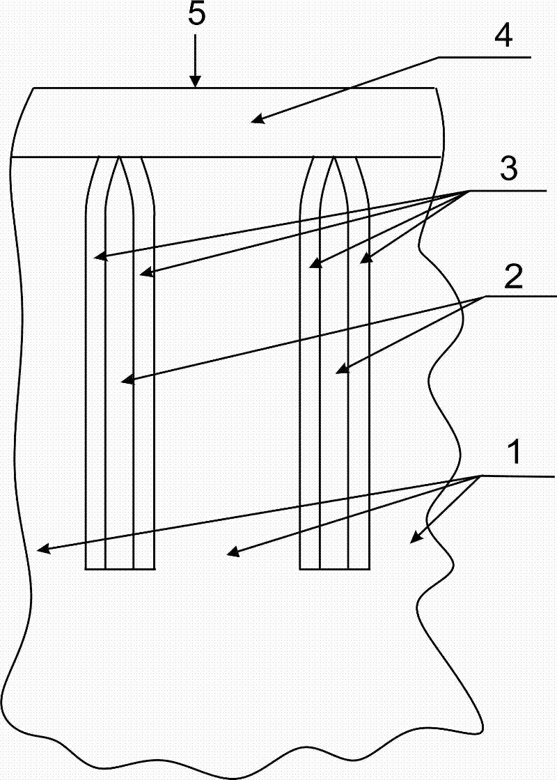
[0028] Step 2. Install the substrate, install the silicon wafer into the electrochemical corrosion tank, the corrosion tank is open, the polished surface, that is, the corrosion surface 5 of the silicon wafer faces in the groove, and keeps light from entering, the back faces outward, and the graphite sheet or metal slice and lead out the electrode wiring;

[0029] Step 3, prepare the solution, mix the concentrated HF acid and the organic solvent in a volume ratio of 1:1 to 1:1.5, and the organic solvent is one of ethanol, propanol, isopropanol, and methanol;

[0030] Step 4. Connect to the power supply, pour the prepared mixed solution into the corrosion tank, the polished surface of the s...

Embodiment 1

[0033] The resistance of the silicon chip is 1 to 10 Ωcm.

[0034] The preparation method is as follows:

[0035] Step 1. Clean the substrate, ultrasonically clean the silicon wafer with acetone, ethanol, and deionized water for 10 minutes respectively, take it out and blow dry;

[0036] Step 2. Install the substrate, install the silicon wafer into the electrochemical corrosion tank, the corrosion tank is open, the polished side faces the tank, and keeps the light entering, the back side faces outward, pad the graphite sheet and lead out the electrode wiring;

[0037] Step 3, prepare solution, mix 48% HF acid and ethanol by volume ratio of 1:1;

[0038] Step 4. Connect the power supply, pour the prepared mixed solution into the corrosion tank, the polished surface of the silicon wafer is in contact with the solution, insert a carbon rod into the solution as an electrode and connect it to the anode, and the electrode on the back of the silicon wafer is connected to the cathode...

Embodiment 2

[0042] The resistance of the silicon chip is 20 to 25 Ωcm.

[0043] The preparation method is as follows:

[0044] Step 1. Clean the substrate, ultrasonically clean the silicon wafer with acetone, ethanol, and deionized water for 10 minutes respectively, take it out and blow dry;

[0045] Step 2. Install the substrate, install the silicon wafer into the electrochemical corrosion tank, the corrosion tank is open, the polished side faces the tank, and keeps the light entering, the back side faces outward, pad the graphite sheet and lead out the electrode wiring;

[0046] Step 3, prepare solution, mix 48% HF acid and ethanol by volume ratio of 1:1.2;

[0047] Step 4. Connect the power supply, pour the prepared mixed solution into the corrosion tank, the polished surface of the silicon wafer is in contact with the solution, insert a carbon rod into the solution as an electrode and connect it to the anode, and the electrode on the back of the silicon wafer is connected to the cathod...


PUM

PropertyMeasurementUnit
sizeaaaaaaaaaa
thicknessaaaaaaaaaa
thicknessaaaaaaaaaa

Abstract

The invention discloses novel porous silicon and a preparation method thereof. The porous silicon has a structure that cylindrical nanometer porous silicon is formed in a low-doped and N-shape monocrystalline silicon film base, and closes straight hole cavities, and the surface is nanometer porous silicon. The invention employs an electrochemical corrosion method, where the structure of the novel porous silicon is made by controlling the mixture solution proportioning and the voltage and current of a dc source in a mixture solution of hydrofluoric acid and an organic solvent. The novel porous silicon structure and the preparation method provide a new technological approach and method for the integration of a silicon-based micro nano device with a sensor, a self-destructing chip, a luminescent device, etc.

Description

technical field [0001] The invention belongs to the technical field of preparation of porous silicon devices and micro-nano structures, and in particular relates to a novel porous silicon and a preparation method thereof. Background technique [0002] Porous silicon nanostructures can be used in a wide range of applications, such as photoluminescent materials, sacrificial layers in microstructure fabrication, gas sensors, biosensors, chip explosive materials, etc. Silicon-based semiconductor devices are gradually developing toward miniaturization and nanotechnology, and the integration of porous silicon, single crystal silicon, and micro-nano devices with small dimensions below the micron level is an important step. [0003] Porous silicon and its preparation methods have been studied for decades. The main method to obtain porous silicon from single crystal silicon is electrochemical corrosion. The corrosion solution is mainly an aqueous solution of HF acid or a mixed soluti...

Claims


Application Information

Patent Timeline
Patent Type & Authority Applications(China)
IPC IPC(8): C30B29/06C30B33/10C25F3/12
Inventor 展长勇任丁邹宇刘波林黎蔚黄宁康
Owner SICHUAN UNIV
Why Eureka
Try Eureka