Silicon-doped bismuth telluride-based memory material for phase-change memory and preparation method of silicon-doped bismuth telluride-based memory material

A storage material, silicon doping technology, applied in the field of microelectronics, can solve the problems of high write current, erase current, amorphous Si resistance, etc., to reduce write current and erase current, small crystalline resistance, and reduce current pulses Effect

Active Publication Date: 2012-04-04
HUAZHONG UNIV OF SCI & TECH
View PDF1 Cites 2 Cited by
  • Summary
  • Abstract
  • Description
  • Claims
  • Application Information

AI Technical Summary

Problems solved by technology

For example, the invention document with the application publication number CN102185106A discloses a SiBiTe-based thin film material for phase-change memory. This material contains a large amount of Si in an amorphous form around the BiTe material, and Si atoms are not incorporated into the BiTe material. , only plays the role of isolation, and only

Method used


Image

  • Silicon-doped bismuth telluride-based memory material for phase-change memory and preparation method of silicon-doped bismuth telluride-based memory material
  • Silicon-doped bismuth telluride-based memory material for phase-change memory and preparation method of silicon-doped bismuth telluride-based memory material
  • Silicon-doped bismuth telluride-based memory material for phase-change memory and preparation method of silicon-doped bismuth telluride-based memory material

Examples


Embodiment 1

[0034] The preparation method of the Si-doped BiTe-based storage material of the present invention can adopt any one of methods such as sputtering method, chemical vapor deposition method, evaporation method, atomic layer deposition method, metal organic compound thermal decomposition method or laser assisted deposition method. A preparation method.

[0035] In the embodiment of this paper, the method of magnetron sputtering is used to prepare Si-doped Bi 2 Te 3 film. First, a Bi with a diameter of 100 mm and a thickness of 5 mm was prepared. 2 Te 3 Target material, the purity of the target is 99.999% (atomic percentage), and the Si sheet with a size of 2*10mm is evenly pasted on the Bi 2 Te 3 On the alloy target, the atomic ratio of Bi to Te is changed by adjusting the sputtering pressure, and the doping amount is changed by changing the number of Si flakes. Then, the method of magnetron sputtering is used, and Ar gas with a purity of 99.999% is introduced during sputte...

Embodiment 2

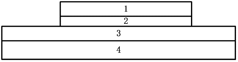
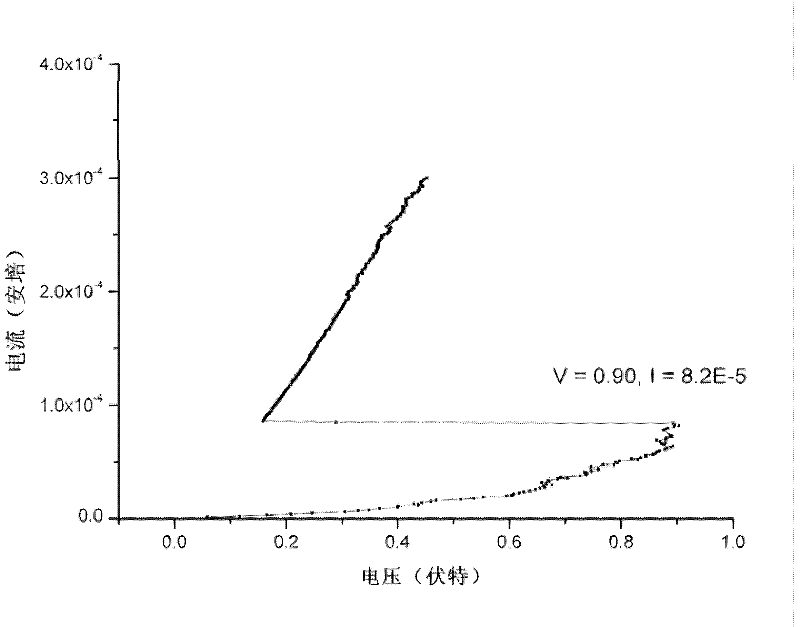
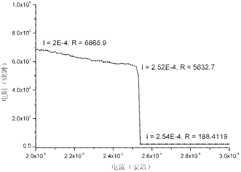
[0038] In order to test the electrical properties of BiTe-based storage materials conveniently, such as figure 1 The simple three-layer structure shown in the figure, 1 is the upper electrode, and 2 is the phase change functional material Bi x Te y Si 100-(x+y) , 3 is the bottom electrode, 4 is the substrate. Among them, the intermediate storage material adopts different compositions of Bi x Te y Si 100-(x+y) film material. The dimensions of each film layer are as follows: the substrate is covered with a layer of SiO 2 thin-film Si sheet; the bottom electrode is TiW with a film thickness of 150nm; the middle is a phase-change functional material with Bi 40 Te 54 Si 6 For example, the thickness is 60nm; the upper electrode is TiW, and the film thickness is 120nm; the plane size of the three-layer structure is 60μm*80μm. Use a probe station to conduct current-voltage (I-V) tests on the three-layer structural unit of the above structure, let the two probes touch the upp...

Embodiment 3

[0041] Bi 40 Te 50 Si 10 , carry out the X-ray diffraction test in the deposited state and after annealing, the test results are as follows Figure 4 shown. In the figure, a is the as-deposited state, and b is the polycrystalline state after annealing at 300°C for 3 minutes. It can be seen from the XRD spectrum that the Si-doped BiTe-based phase-change memory material exhibits a single triangular structure in the crystalline state.


PUM

PropertyMeasurementUnit
Diameteraaaaaaaaaa
Thicknessaaaaaaaaaa
Film thicknessaaaaaaaaaa

Abstract

The invention provides a silicon-doped bismuth telluride-based memory material for a phase-change memory and a preparation method of the silicon-doped bismuth telluride-based memory material. A chemical formula of the silicon-doped bismuth telluride-based material is BixTeySi100 minus (x plus y), wherein the x and the y satisfy the following conditions that the x is more than 0 and is less than or equal to 40, the y is more than 0 and is less than or equal to 60, and the x plus the y is more than or equal to 90 and is less than 100. Under the situation that an electrical impulse signal is applied, the silicon-doped bismuth telluride-based material has the reversible characteristic between a high-impedance state and a low-impedance state and can be used for the phase-change memory. Compared with the traditional GeTe, SiSbTe, GeSbTe and other phase-change thin-film materials for the phase-change memory, the silicon-doped bismuth telluride-based material has simple component, quicker phase-change speed, lower energy required for phase change and good compatibility with a complementary metal oxide semiconductor (CMOS) device manufacturing process, and is an excellent new memory material for the phase-change memory.

Description

technical field [0001] The invention belongs to the field of microelectronics, and in particular relates to a phase-change storage material which can be used in a phase-change storage and a preparation method thereof. Background technique [0002] Higher density, lower power consumption, lower cost and faster speed are the eternal goals pursued by memory designers and manufacturers. In the existing storage technology, phase change memory (PCRAM) is characterized by high-speed reading, high rewritable times, radiation resistance, non-volatility, small component size, multi-level storage, and compatibility with CMOS processes. With good advantages, it is considered by the International Semiconductor Industry Association that it is most likely to replace the current flash memory and become one of the mainstream products of future memory, and it is also the first next-generation memory device that may be commercialized. [0003] Phase change memory technology is based on Ovshin...

Claims


Application Information

Patent Timeline
IPC IPC(8): H01L45/00C22C12/00
CPCC22C1/10H01L45/06C22C12/00H01L45/148C22C28/00H01L45/00H10N70/231H10N70/884
Inventor 程晓敏鞠晨缪向水
Owner HUAZHONG UNIV OF SCI & TECH
Why Eureka
Try Eureka