Method for preparing large-grain ingot polycrystal silicon

A large-grain, polysilicon technology, applied in the field of preparing large-grain ingot polysilicon, can solve the problems of narrow process window, unfavorable large-scale promotion, inability to induce polycrystalline growth, etc., and achieve the effect of coarse grains

Inactive Publication Date: 2012-04-25
TRINA SOLAR CO LTD
View PDF7 Cites 12 Cited by
  • Summary
  • Abstract
  • Description
  • Claims
  • Application Information

AI Technical Summary

Problems solved by technology

[0005] The technical problems to be solved by the present invention are: (1) the cost of the single crystal seed crystal used is relatively high; (2) the seed crystal does not melt at all or all of the melting can not play the role of inducing polycrystalline growth, and the process window is narrow, which is not conducive to the industry. Timely large-scale promotion

Method used


Image

  • Method for preparing large-grain ingot polycrystal silicon
  • Method for preparing large-grain ingot polycrystal silicon

Examples


Embodiment 1

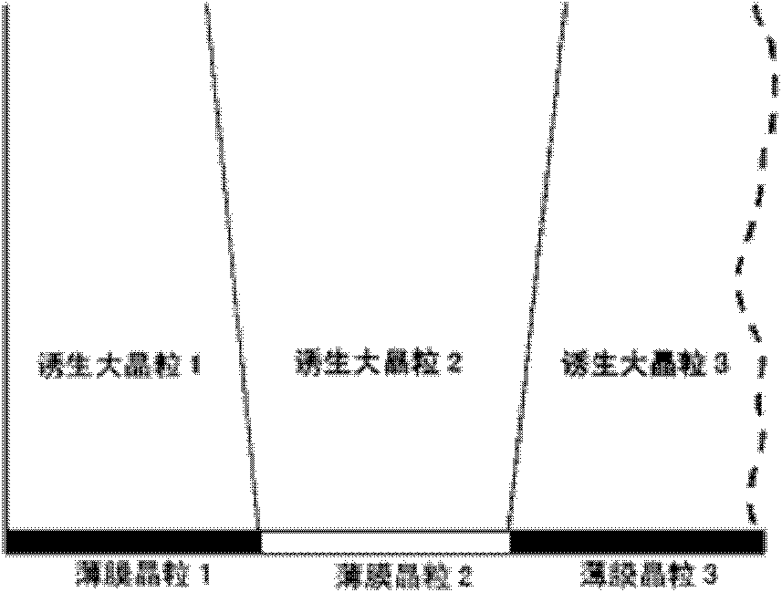
[0031] Embodiment 1. A silicon carbide film was placed on the bottom of a quartz crucible sprayed with a silicon nitride release agent. The thickness of the silicon carbide film was 80 μm, and the average grain size of the silicon carbide film was 100 mm. After charging 450 kg of silicon material into the crucible, the crucible was loaded into a furnace. The furnace is evacuated, and Ar is used as the protective gas. Design the thermal field so that the temperature of the silicon material in the furnace is higher than 1420°C but lower than 1480°C, so that the silicon material is completely melted, and the silicon carbide film will not melt because of its high melting point (>2800°C). After the silicon material is fully melted, open the insulation cover, adjust the thermal field, gradually solidify from the bottom of the crucible, rely on the induction of large grains of silicon carbide film to achieve directional growth of silicon crystals, and obtain large grain castings with...

Embodiment 2

[0033] Example 2. A boron nitride film was placed on the bottom of a quartz crucible sprayed with a silicon nitride release agent. The thickness of the boron nitride film was 60 μm, and the average grain size of the boron nitride film was 150 mm. After charging 450 kg of silicon material into the crucible, the crucible was loaded into a furnace. The furnace is evacuated, and Ar is used as the protective gas. Design the thermal field so that the temperature of the silicon material in the furnace is higher than 1420°C but lower than 1480°C, so that the silicon material is completely melted, and the boron nitride film will not melt because of its high melting point (>2900°C). After the silicon material is fully melted, open the heat preservation cover, adjust the thermal field, gradually solidify from the bottom of the crucible, rely on the induction of large grains of boron nitride film to achieve directional growth of silicon crystals, and obtain large grains with an average gr...

Embodiment 3

[0035] Example 3. A tantalum carbide film was placed on the bottom of a quartz crucible sprayed with a silicon nitride release agent. The thickness of the tantalum carbide film was 50 μm, and the average grain size of the boron nitride film was 250 mm. After charging 450 kg of silicon material into the crucible, the crucible was loaded into a furnace. The furnace is evacuated, and Ar is used as the protective gas. Design the thermal field so that the temperature of the silicon material in the furnace is higher than 1420°C but lower than 1480°C, so that the silicon material is completely melted, and the tantalum carbide film will not melt because of its high melting point (>3600°C). After the silicon material is fully melted, open the insulation cover, adjust the thermal field, gradually solidify from the bottom of the crucible, rely on the induction of large grains of tantalum carbide film to realize the directional growth of silicon crystals, and obtain large grain castings w...


PUM

PropertyMeasurementUnit
melting pointaaaaaaaaaa
depthaaaaaaaaaa
areaaaaaaaaaaa

Abstract

The invention relates to a method for preparing large-grain ingot polycrystal silicon. The directional growth of polycrystal silicon grains is induced by adopting a large-grain film with a high melting point in the method. The large-grain film is made of metallic high-purity oxide, nitride, nitric oxide, carbide or boride, or high-purity silicon nitride, boron nitride, silicon carbide or boron carbide; the melting point is more than 1,480 DEG C, the purity is more than or equal to 99.9 percent, the thickness of the film is 0.01 to 500 mu m, and the diameter of the grains is 10 to 400 mm; and in the horizontal direction, the crystal face of the grains can be effectively matched with a certain crystal face of the crystal silicon, so that the growth of the crystal silicon grains is induced. The ingot polycrystal silicon crystal prepared by the method has the characteristic of thick grains, the average granularity of the grains is more than 20 mm, the service life of minority carriers of a silicon chip is over 30 percent longer than that of the ingot polycrystal prepared by adopting the same ingot casting technology and grown without film induction, and the absolute value of the conversion efficiency of a photovoltaic cell sheet prepared from the ingot polycrystal silicon is 0.5 to 1.5 percent higher than that of the ingot polycrystal silicon prepared by adopting the same ingot casting technology and grown without film induction.

Description

technical field [0001] The invention relates to a method for preparing large-grain ingot polysilicon. Background technique [0002] Ingot polycrystalline has gradually become the mainstream in the field of crystalline silicon photovoltaic cells due to its low cost advantages. However, there are a large number of micro-defects in the ingot polysilicon, such as grain boundaries and dislocations. Such micro-defects have an atomic arrangement different from the perfect crystal periodic structure, and as electroactive centers, they significantly affect the minority carrier recombination life of polysilicon, making the photoelectric conversion efficiency of polysilicon photovoltaic cells 1-2% lower than that of single-crystal silicon. [0003] At present, the inner wall of ordinary quartz crucible used for polysilicon ingot is sprayed with release agent boron nitride. When the silicon melt is directional solidified, the grain growth tends to be randomly distributed. The grain siz...

Claims


Application Information

Patent Timeline
Patent Type & Authority Applications(China)
IPC IPC(8): C30B29/06C30B28/06
Inventor 熊震付少永张驰王梅花
Owner TRINA SOLAR CO LTD
Why Eureka
Try Eureka