Negative photoresist-based diffuser photo-etching process

A technology of negative photoresist and photolithography process, which is applied in the field of negative photoresist photolithography process and diffusion sheet photolithography process based on negative photoresist, which can solve the problem of uneven doping and uncontrollable light field. , uneven light field and other problems, to achieve the effect of simple preparation process, reduced device cost, and little effect of ultraviolet light

Inactive Publication Date: 2012-06-27
SOUTHEAST UNIV
View PDF5 Cites 23 Cited by
  • Summary
  • Abstract
  • Description
  • Claims
  • Application Information

AI Technical Summary

Problems solved by technology

The former is currently widely used in flat panel displays, but its transmittance is low, the light field is uncontrollable, and due to the uneven doping, the light field is not uniform

Method used


Image

  • Negative photoresist-based diffuser photo-etching process
  • Negative photoresist-based diffuser photo-etching process
  • Negative photoresist-based diffuser photo-etching process

Examples


Embodiment 1

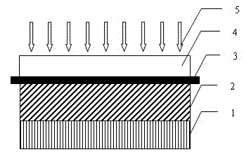
[0065] Fabrication of SU-8 Negative Photoresist Grooves on Monocrystalline Silicon Wafers

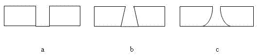
[0066] Firstly, SU-8 photoresist 2 is spin-coated on a single-side polished single-crystal silicon wafer substrate 1, then pre-baked on a hot plate, and cooled naturally to room temperature. Then place the diffuser 4 on the mask plate 3, use a photolithography machine to perform ultraviolet contact exposure, then pre-baked on a hot plate, and finally develop in the developer solution PMGEA to obtain the SU-8 negative photo Resist grooves such as Figure 5 As shown, some of its cross-sectional lines are as Figure 4 shown.

Embodiment 2

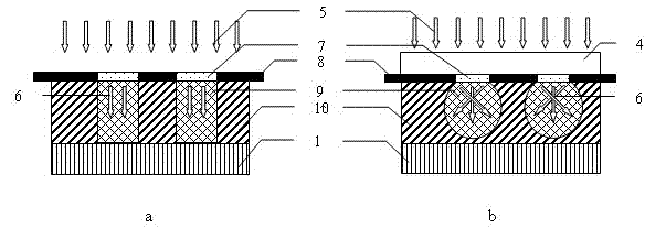
[0068] Fabrication of NR9-3000PY negative photoresist photonic crystal on K9 optical glass

[0069] First, NR9-3000PY photoresist 2 was spin-coated on a K9 optical glass substrate 1, then pre-baked on a hot plate, and cooled to room temperature naturally. Then place the diffusion sheet 4 on the mask plate 3, use a photolithography machine to perform ultraviolet contact exposure, then pre-bake on a hot plate, and finally develop in the developer solution R6 to obtain the obtained NR9-3000PY negative photo Resist photonic crystal unit such as Figure 6 As shown, a part of its cross-section is shown as Figure 4 As shown, the negative photoresist columns and negative photoresist wells can be produced due to the difference of the mask plate, and the photonic crystal such as Figure 7 shown. )

[0070] According to the graphic cross-section lines made in embodiment 1 and embodiment 2, the exposure process of the diffuser negative photoresist lithography proposed by the present ...


PUM


Abstract

The invention relates to a negative photoresist-based diffuser photo-etching process, which comprises the following steps that: firstly, photoresist is coated on the surface of an underlay, then the underlay which is coated with the negative photoresist in a rotating way is prebaked so as to remove solvent of the negative photoresist; then exposure is carried out, a diffuser is arranged on a mask plate, and the diffuser and the mask plate are used as a mask to perform ultraviolet exposure on the negative photoresist; finally the post-baking and developing are carried out, the negative photoresist in an exposure area is cross-linked in the post-baking process and is free from being dissolved in developing liquid, and a structure with a particular cross section is obtained; and the diffuser and the mask plate are collectively used as the mask to anticipate the exposure of the photoresist. The negative photoresist-based diffuser photo-etching process has advantages of wide application range, simple technique process, good technical repeatability, unnecessary modification of present photo-etching equipment, low cost, easiness in mass production and the like.

Description

technical field [0001] The present invention relates to a photolithography process method in the field of semiconductor technology, micro-electromechanical system (MEMS) field and integrated optics field, in particular to a diffusion sheet photolithography process method based on negative photoresist, more precisely, a simultaneous A negative-tone photoresist lithography process that uses a diffuser and a mask as a lithography mask. Background technique [0002] Photolithography plays a pivotal role in the fabrication of integrated optoelectronic devices. The photolithography process usually refers to the precise copying of the pattern of the photolithographic mask onto the photoresist coated with the surface of the material to be etched by photocopying. Lithography plays a pivotal role in the manufacturing process of integrated optical devices, MEMS and integrated circuit chips (IC). Lithography has been widely regarded as one of the key technologies for mass-manufacturing...

Claims


Application Information

Patent Timeline
Patent Type & Authority Applications(China)
IPC IPC(8): G03F7/20G03F7/00G02B5/02
Inventor 张彤李若舟张晓阳
Owner SOUTHEAST UNIV
Why Eureka
Try Eureka