Cuprous oxide-based PIN-junction solar battery of nano structure and preparation method thereof
A cuprous oxide-based, solar cell technology, applied in the field of solar cells, can solve the problems of ineffective separation and collection of photo-generated carriers, inability of built-in electric field separation of photo-generated carriers, and reduction of photosensitive sensitivity of solar cells, etc. The effect of improving photoelectric conversion efficiency, abundant storage capacity, and increasing width
- Summary
- Abstract
- Description
- Claims
- Application Information
AI Technical Summary
Problems solved by technology
Method used
Image
Examples
Embodiment 1
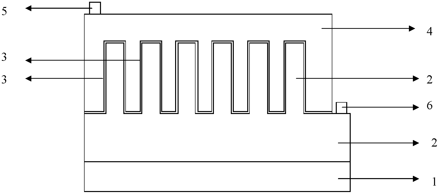
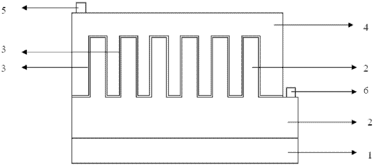
[0045] Preparation of cuprous oxide-based PIN junction solar cells with nanostructures, such as figure 1 shown, including the following steps:
[0046] (1) Cleaning the substrate 1: take the glass deposited with a 180nm ITO transparent conductive film as the substrate 1, and ultrasonically clean it in acetone, ethanol, and deionized water for 10 minutes respectively, and use N 2 blow dry.
[0047] (2) Grow P-type cuprous oxide nanowire array 2 on substrate 1 by electrochemical deposition method: use three-electrode method to prepare 0.003mol / L Cu(NO 3 ) 2 and 0.5mol / L KCl aqueous solution, using the substrate 1 cleaned in step (1) as the working electrode, using Ag / AgCl reference electrode and platinum wire counter electrode, and galvanostatic deposition at 60°C for 1h to obtain P Type cuprous oxide nanowire array 2 with a diameter of 50 nm and a length of 0.5 μm.
[0048] (3) Growth insulating layer 3: Deposit a layer of high-resistance zinc oxide on the surface of the P-ty...
Embodiment 2
[0053] Preparation of cuprous oxide-based PIN junction solar cells with nanostructures, such as figure 1 shown, including the following steps:
[0054] (1) Clean the substrate 1: take the glass deposited with a 200nm FTO transparent conductive film as the substrate 1, and then ultrasonically clean it in acetone, ethanol, and deionized water for 15 minutes respectively, and use N 2 blow dry.
[0055] (2) Grow P-type cuprous oxide nanowire array 2 on substrate 1 by electrochemical deposition: use three-electrode method to prepare 0.004mol / L Cu(NO 3 ) 2 and 1mol / L KCl aqueous solution, using the substrate 1 cleaned in step (1) as the working electrode, using the Ag / AgCl reference electrode and the platinum wire counter electrode, and depositing at 70°C for 3 hours by constant current method to obtain P-type The cuprous oxide nanowire array 2 has a diameter of 200 nm and a length of 1.5 μm.
[0056] (3) Growth insulating layer 3: Deposit a layer of high-resistance titanium dio...
PUM
| Property | Measurement | Unit |
|---|---|---|
| diameter | aaaaa | aaaaa |
| length | aaaaa | aaaaa |
| electrical resistivity | aaaaa | aaaaa |
Abstract
Description
Claims
Application Information

