Method and device for processing nano structures by utilizing controllable pulse lasers

A pulsed laser and nanostructure technology, applied in microstructure devices, manufacturing microstructure devices, nanotechnology, etc., can solve the problems of difficult promotion, high cost, and difficult control, and achieve good application effects, simple methods, and easy industrialization. Effect

Inactive Publication Date: 2012-07-18
GUIZHOU UNIV
View PDF8 Cites 7 Cited by
  • Summary
  • Abstract
  • Description
  • Claims
  • Application Information

AI Technical Summary

Problems solved by technology

[0003] At present, the common traditional technologies for the preparation and processing of luminescent materials and compone

Method used


Image

  • Method and device for processing nano structures by utilizing controllable pulse lasers
  • Method and device for processing nano structures by utilizing controllable pulse lasers
  • Method and device for processing nano structures by utilizing controllable pulse lasers

Examples


Embodiment 1

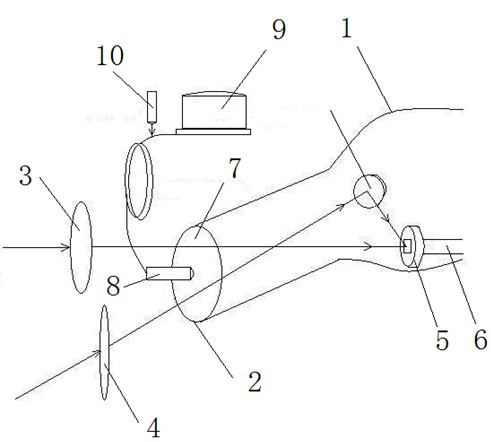
[0021] Embodiment 1 of the present invention: the structure of a device for processing nanostructures using a controllable pulsed laser is as follows figure 1 As shown, a vacuum chamber 1 is included, a laser window 2 is provided on the side of the vacuum chamber 1, a cavity incident mirror 7 is provided on the laser window 2, a PLE laser lens 3 is provided outside the laser window 2, and a laser window 2 is provided on the side of the vacuum chamber 2. 1 is provided with a sample stage 5, the sample stage 5 corresponds to the optical path of the PLE laser lens, and a sampling handle 6 is connected to the rear end of the sample stage 5; A spectrometer 9 is provided, and an optical fiber probe 8 is connected to the spectrometer 9; a PLD laser lens 4 is provided outside the laser window 2, and a target platform 7 is provided in the vacuum cavity 1, and the target platform 7 corresponds to the optical path of the PLD laser lens 4; The probe 8 is a bidirectional optical fiber prob...

Embodiment 2

[0023] Embodiment 2 of the present invention: a method for processing nanostructures using a controllable pulse laser, placing a P-type single crystal silicon wafer on the sample stage 5, and installing a silicon target on the target stage 7, in the vacuum chamber 1 Vacuum up to 10 -5 Pa, and then control the multi-gas path of the vacuum chamber 1 to make the sample in a nitrogen atmosphere environment, select a nanosecond pulse laser head with a wavelength of 532nm, and install the PLE laser lens 3 and PLD laser lens 4 corresponding to the wavelength , so that the nanosecond pulsed laser head emits pulsed laser light, enters the vacuum cavity 1 from the laser window 2 through the PLE laser lens 3, and then converges on the surface of the P-type single crystal silicon wafer to etch the P-type single crystal silicon wafer. During the processing, the optical fiber probe 8 is used to detect the change of the electronic spectrum in the plasma glow generated by the pulse laser acti...

Embodiment 3

[0024] Embodiment 3 of the present invention: using a method for processing nanostructures with a controllable pulse laser, the semiconductor substrate sample is placed on the sample stage 5, and the silicon target is installed on the target stage 7, and vacuum is drawn in the vacuum chamber 1 , draw up to 10 -5Pa, and then control the multiple gas channels of the vacuum chamber 1 to make the sample in an oxygen atmosphere environment, select a nanosecond pulse laser head with a wavelength of 1064nm, and install the PLE laser lens 3 and PLD laser lens 4 corresponding to the wavelength , so that the nanosecond pulse laser head emits pulsed laser light, the pulsed laser light enters the vacuum cavity 1 from the laser window 2 through the PLE laser lens 3, and then converges on the sample surface for etching processing; during the processing, the optical fiber probe 8 Detect changes in the electronic spectrum in the plasma glow generated by the pulsed laser on the sample to contr...


PUM


Abstract

The invention discloses a method and a device for processing nano structures by utilizing controllable pulse lasers. By means of the method for processing nano structures by utilizing the controllable pulse lasers, the pulse lasers emitted by a pulse laser head enter into a vacuum cavity through a pulse laser etching (PLE) laser lens and converge on the surface of a sampler in the vacuum cavity to process the sampler; and the pulse lasers are regulated and controlled to etch various luminous nano structures by utilizing changes of an electronic spectrum in plasma glow generated by online detection of a fiber-optic probe and controlling oscillation frequency of a plasma wave by changing processing atmospheres. The method and the device utilize the pulse laser plasma etching technology, utilize the fiber-optic probe to detect changes of the plasma glow in different atmospheres, and obtain controllable activation operation on luminous operation materials through change of the processing atmospheres. The method and the device can achieve composite processing of the PLE and the pulse laser deposition (PLD) by switching light paths, manufacture luminous nano structures of various semi-conductors, and especially manufacture superlattice luminous structures containing quantum dots.

Description

technical field [0001] The invention relates to a method and a device for processing semiconductor materials by using a laser, in particular to a method and a device for processing a nanostructure by using a controllable pulse laser. Background technique [0002] The development of today's information photonization has entered the integration of optoelectronics on the chip and all-opticalization at the chip level. bottleneck work. In addition, it is imperative to let semiconductor light emitting and lighting into thousands of households, which is the demand of low carbon and environmental protection. At present, there is an urgent need for the preparation and processing technology of high-brightness luminescent materials and components. [0003] At present, the common traditional technologies for the preparation and processing of luminescent materials and components are molecular beam epitaxy (MBE) technology and chemical vapor deposition (CVD) technology. promoted to ind...

Claims


Application Information

Patent Timeline
IPC IPC(8): B81C1/00B82Y40/00B23K26/36B23K26/12B23K26/362
Inventor 黄伟其
Owner GUIZHOU UNIV
Why Eureka
Try Eureka