Preparation method of gallium nitride self-supporting substrate
A self-supporting substrate and supporting substrate technology, applied in semiconductor/solid-state device manufacturing, electrical components, nanotechnology, etc., can solve the problems of high dislocation density of epitaxial materials and uneven distribution of nanoscale patterned substrates, etc. Achieve the effect of low requirements for preparation conditions, improve availability, and reduce dislocation density
- Summary
- Abstract
- Description
- Claims
- Application Information
AI Technical Summary
Problems solved by technology
Method used
Image

Examples
preparation example Construction
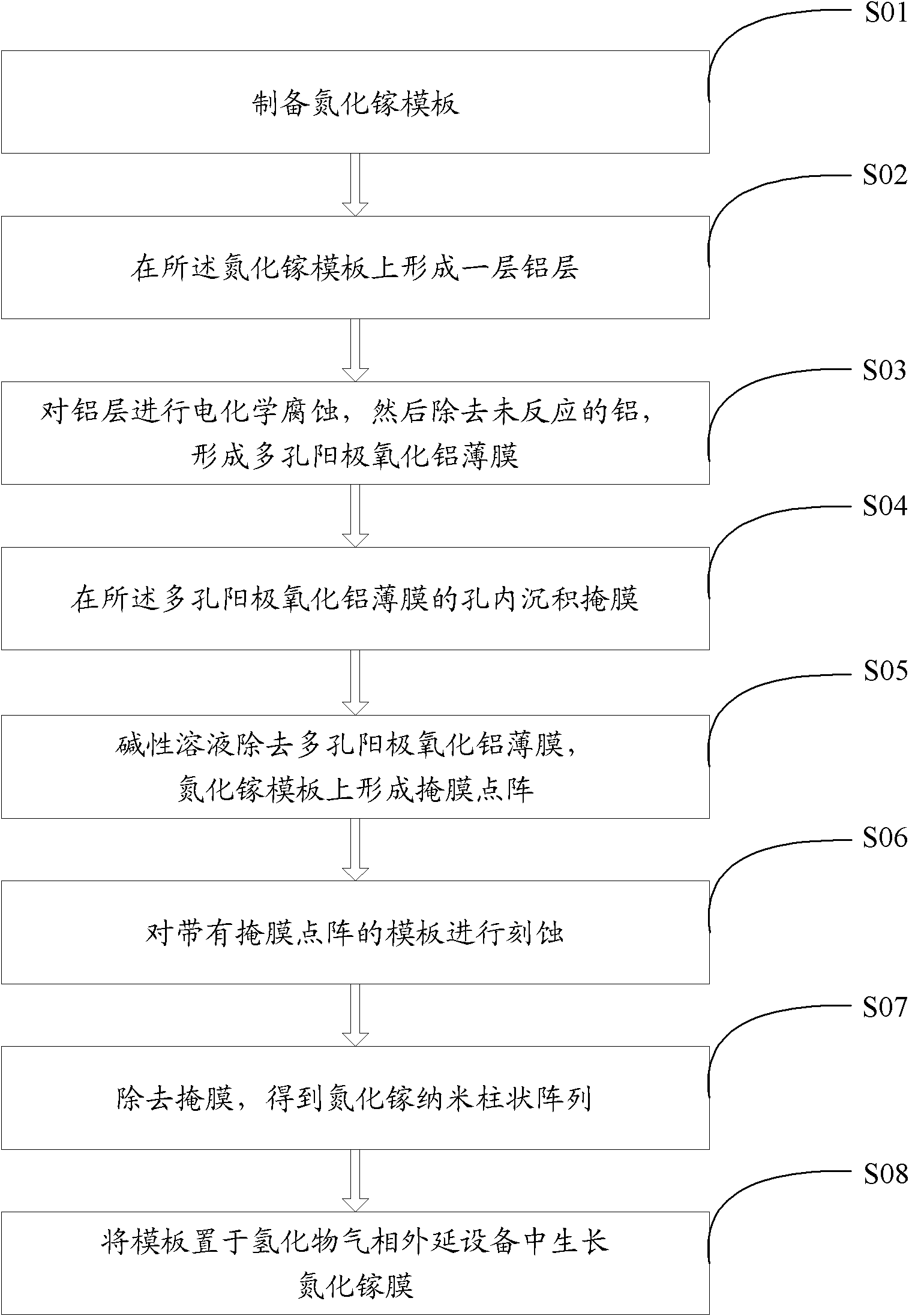
[0018] see figure 1 , showing a method for preparing a GaN self-supporting substrate according to an embodiment of the present invention, the method comprising the following steps:
[0019] S01: preparing a GaN template;
[0020] S02: forming an Al layer on the GaN template;
[0021] S03: electrochemically corroding the Al layer to form an AAO film;
[0022] S04: Depositing a mask into the pores of the AAO film;
[0023] S05: removing the AAO film, and forming a mask lattice on the GaN template;
[0024] S06: Etching the GaN template with mask lattice;
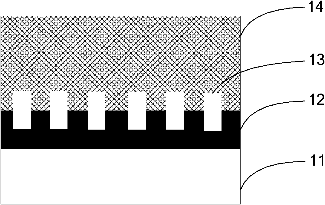
[0025] S07: removing the mask to obtain a GaN nano-pillar array;
[0026] S08: growing a GaN film on the GaN nano-pillar array.
[0027] In step S01, the GaN template is formed by growing GaN on a heteroepitaxial substrate, and the heteroepitaxial substrate is Al 2 o 3 , SiC, Si, or any one of GaAs; the growth method of growing a layer of GaN on the heteroepitaxial substrate can be HVPE, metal organic chemical vapor de...
Embodiment 1
[0040] Using MOCVD method in Al 2 o 3 A GaN film of about 3 μm was grown on the (0001) surface of the substrate, and this film was used as a HVPE template. At a temperature of 200 ° C, a 300 nm thick metal Al thin layer was deposited on the surface of the template by electron beam evaporation. Put the template with Al layer into oxalic acid solution (0.3mol / L), anodize at room temperature with a voltage of 40V for about 15min, at this time the metal Al is electrochemically corroded into porous AAO with regular distribution, and place the template at 30°C Soak in 5wt% phosphoric acid solution for 40min, after cleaning, electron beam deposition of 20nm thick Ni in the nanopore, and then use 0.2mol / L NaOH to remove the anodic aluminum oxide, then obtain metallic Ni nanoscale on the GaN template Lattice; put the template into an ICP reaction chamber for etching, remove metal Ni with a mixed solution of nitric acid: hydrofluoric acid = 1:3, and obtain a GaN nano columnar array. F...
Embodiment 2
[0042] Using the HVPE method in Al 2 o 3 A GaN film of about 3 μm was grown on the substrate (0001), and this film was used as a HVPE template. At a temperature of 200 ° C, a 400-nm-thick metal Al thin layer was deposited on the surface of the template by electron beam evaporation. Put the template with Al layer into oxalic acid solution (0.3mol / L), anodize at room temperature with a voltage of 40V for about 20min, at this time the metal Al is electrochemically corroded into porous AAO with regular distribution, and place the template at 30°C Soak in 5wt% phosphoric acid solution for 50min, after cleaning, electron beam deposit 25nm thick Ni in the nanopore, and then use 0.2mol / L NaOH to remove the anodic aluminum oxide, then obtain metal Ni nanoscale on the GaN template Lattice; put the template into the RIE reaction chamber for etching, and remove metal Ni with a mixed solution of nitric acid: hydrofluoric acid = 1:3 to obtain a GaN nano-columnar array. Finally, the GaN co...
PUM
| Property | Measurement | Unit |
|---|---|---|
| Thickness | aaaaa | aaaaa |
| Thickness | aaaaa | aaaaa |
| Thickness | aaaaa | aaaaa |
Abstract
Description
Claims
Application Information
 - R&D
- Intellectual Property
- Life Sciences
- Materials
- Tech Scout
- Unparalleled Data Quality
- Higher Quality Content
- 60% Fewer Hallucinations
Browse by: Latest US Patents, China's latest patents, Technical Efficacy Thesaurus, Application Domain, Technology Topic, Popular Technical Reports.
© 2025 PatSnap. All rights reserved.Legal|Privacy policy|Modern Slavery Act Transparency Statement|Sitemap|About US| Contact US: help@patsnap.com