
Method for improving doping uniformity among silicon carbide multilayer structure epitaxial material batches

A technology of epitaxial materials and multi-layer structures, which is applied in the fields of electrical components, semiconductor/solid-state device manufacturing, circuits, etc., can solve problems such as strong background memory effect, reduced production capacity, and lattice loss, so as to reduce background memory effect and improve repetition performance, improve precise and controllable effect

Active Publication Date: 2014-09-24
NO 55 INST CHINA ELECTRONIC SCI & TECHNOLOGYGROUP CO LTD +1
View PDF4 Cites 0 Cited by
  • Summary
  • Abstract
  • Description
  • Claims
  • Application Information

AI Technical Summary

Problems solved by technology

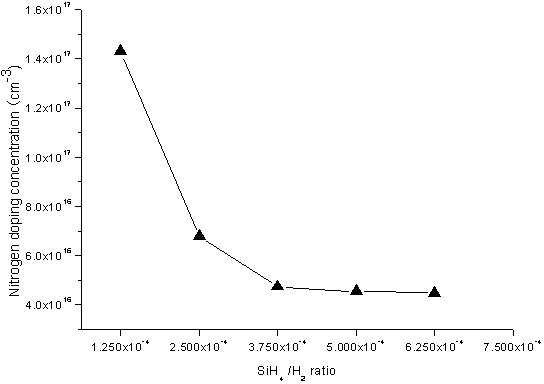
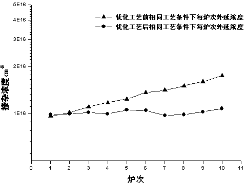
[0003] The epitaxial materials used in silicon carbide power electronic devices are generally composed of multi-layer epitaxial layers, such as silicon carbide Schottky barrier diode structure epitaxial materials, in order to ensure high blocking voltage, high-resistance thick-layer epitaxy is required, and at the same time, in order to alleviate N + Due to the lattice mismatch caused by the difference in doping concentration between the substrate and the high-resistance thick-layer epitaxy, a buffer layer needs to be added between the substrate and the high-resistance thick-layer epitaxy; at a high epitaxy rate, the required doping of the buffer layer can be achieved. It is necessary to increase the nitrogen flow rate, which will cause a strong background memory effect; under the same epitaxial process conditions, the doping concentration of the epitaxial material channel layer will gradually increase with the number of furnaces, resulting in batch-to-batch doping Concentration uniformity is reduced; if the memory effect is to be eliminated, a long time of baking is required, resulting in longer process time and lower production capacity

Method used

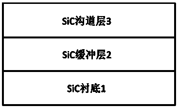

Image

  • Method for improving doping uniformity among silicon carbide multilayer structure epitaxial material batches
  • Method for improving doping uniformity among silicon carbide multilayer structure epitaxial material batches
  • Method for improving doping uniformity among silicon carbide multilayer structure epitaxial material batches

Examples


Embodiment 1

[0026] The provided method for epitaxially growing a 600V Schottky diode structure epitaxial material on a (0001) silicon surface silicon carbide substrate with an 8° bias to the direction includes the following steps:

[0027] 1) Select the (0001) silicon surface 4H-SiC conductive substrate for epitaxial growth with an angle of 8° to the direction, and place the substrate on a graphite base coated with tantalum carbide;

[0028] 2) The system is heated up to 1400°C, and the pressure is set to 100mbar, and the substrate surface is treated online under the atmosphere of hydrogen (flow 80L / min), argon (flow 3L / min) and propane (flow 10ml / min) to remove the surface damage and contamination, the treatment time is the time required for the temperature to rise from 1400°C to the actual growth temperature of 1570°C;

[0029] 3) The temperature is stabilized at 1570°C, the set pressure is 100mbar, the flow rates of silane and propane are 10ml / min and 3.5ml / min respectively, the carb...

Embodiment 2

[0037] The provided method for epitaxially growing 1200V JFET epitaxial materials on a (0001) silicon surface silicon carbide substrate with an 8° bias to the direction includes the following steps:

[0038] 1) Select the (0001) silicon surface 4H-SiC conductive substrate for epitaxial growth with an angle of 8° to the direction, and place the substrate on a graphite base coated with tantalum carbide;

[0039] 2) The system is heated up to 1400°C, and the pressure is set to 100mbar, and the substrate surface is treated online under the atmosphere of hydrogen (flow 80L / min), argon (flow 3L / min) and propane (flow 10ml / min) to remove the surface damage and contamination, the treatment time is the time required for the temperature to rise from 1400°C to the actual growth temperature of 1570°C;

[0040] 3) The temperature is stabilized at 1570°C, the set pressure is 100mbar, the flow rates of silane and propane are 20ml / min and 10ml / min respectively, the carbon-silicon ratio at t...


PUM

PropertyMeasurementUnit
thicknessaaaaaaaaaa
thicknessaaaaaaaaaa
thicknessaaaaaaaaaa

Abstract

The invention relates to a method for improving doping uniformity among silicon carbide multilayer structure epitaxial material batches, which includes that a chemical vapor phase deposition growth technology serves as the base, pure silane and pure propane serve as growth sources, hydrogen gas serves as carrier gas and diluent gas, and nitrogen gas serves as a doping agent to achieve n-type dopping after a (0001) silicon surface carbonized silicon substrate which inclines to a direction (11-20) by 8 degrees is preprocessed. Nitrogen gas doping efficiency is increased by using low speed epitaxy method and combing carbon and silicon ratio at a low air inlet end, a thin epitaxial layer with high doping concentration is grown on the carbonized silicon substrate in an epitaxial mode by using lower nitrogen gas flow, when a high resistance thick layer epitaxy is grown, the C / Si ration at an air inlet end is increased, and channel layers with the needed concentration and thickness are grown by using high speed epitaxy method to reduce background memory effects. The method has the advantages that repeatability of epitaxy technique is improved, and technical support is provided for batch production of silicon carbide multilayer structure epitaxial materials and particularly Schottky diode structure epitaxial materials.

Description

technical field [0001] The invention proposes a method for improving the doping uniformity between batches of silicon carbide multilayer structure epitaxial materials, and improves the repeatability of the epitaxial process. It belongs to the technical field of semiconductor materials. Background technique [0002] Power electronics technology is the core technology in the field of energy and electric energy conversion. High-efficiency energy conversion is an important driving force for energy saving, environmental protection, and low-carbon economy. High-voltage and large-capacity power electronic devices for high-efficiency energy conversion are key components and foundations; long-term Silicon devices have been dominant in almost all applications of power electronic systems since the beginning; there is no doubt that mature process technology is the biggest advantage of silicon devices; however, the performance of silicon devices is close to the theoretical limit determin...

Claims


Application Information

Patent Timeline
Patent Type & Authority Patents(China)
IPC IPC(8): H01L21/205
Inventor 李赟尹志军朱志明马林宝
Owner NO 55 INST CHINA ELECTRONIC SCI & TECHNOLOGYGROUP CO LTD
Learn More