Method improving manufacturing process of crystalline silicon solar cell through arsenic ion implantation

A solar cell, ion implantation technology, applied in sustainable manufacturing/processing, circuits, electrical components, etc., can solve problems such as reducing minority carrier lifetime and battery efficiency, increasing surface recombination rate, increasing surface density of states, etc., to achieve large-scale The effect of mass production, improvement of minority carrier lifetime, and reduction of surface density of states

Active Publication Date: 2012-09-19
SUZHOU INST OF NANO TECH & NANO BIONICS CHINESE ACEDEMY OF SCI
View PDF4 Cites 4 Cited by
  • Summary
  • Abstract
  • Description
  • Claims
  • Application Information

AI Technical Summary

Problems solved by technology

But this will also bring other problems. On the one hand, high-concentration phosphorus implantation will generate a large number of defects on the silicon surface, increasing the surface state density, thereby increasing the surface recombination rate, reducing the minority carrier lifetime and cell efficiency.
On the other hand, the implanted junction depth and concentration need to meet the ohmic contact between the metal on the battery surface and the silicon wafer at the same time. The very mature screen printing and sintering process conditions in the industry cannot be directly applied, and the process conditions need to be explored separately.

Method used


Image

  • Method improving manufacturing process of crystalline silicon solar cell through arsenic ion implantation
  • Method improving manufacturing process of crystalline silicon solar cell through arsenic ion implantation

Examples


Embodiment

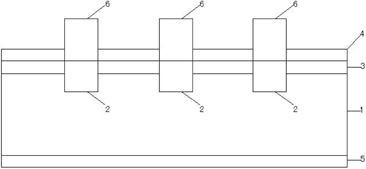
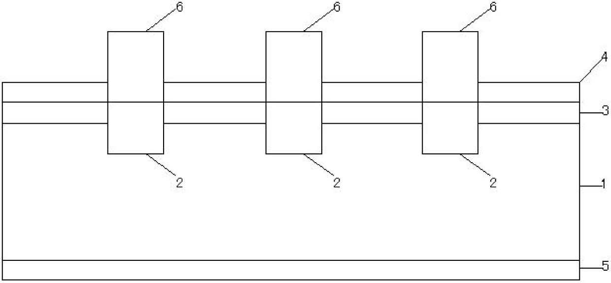
[0031] This embodiment describes a crystalline silicon solar cell formed by ion-implanting arsenic, which includes, from the front to the back (the front refers to the light-receiving surface, and the back refers to the non-light-receiving surface) sequentially: a silver metal positive electrode 6 on the front, nitrogen Silicone anti-reflection film 4, n+ region 3 formed by ion implantation of arsenic on the front (hereinafter referred to as n+ region 3), n+ diffusion layer 2 formed by diffusion of phosphorus in the designated region on the front, silicon substrate 1 and aluminum back electric field 5 on the back.

[0032] The specific manufacturing process steps are as follows:

[0033] Performing damage removal and surface texturing on the P-type crystalline silicon substrate 1;

[0034] A patterned diffusion junction is performed on a designated area on the front side of the silicon substrate 1 . Deposit silicon oxide or silicon nitride on the front side of the silicon sub...


PUM


Abstract

The invention discloses a method improving a manufacturing process of a crystalline silicon solar cell through arsenic ion implantation. On one hand, an N-type area is formed on the surface of the crystalline silicon solar cell through arsenic ion implantation, the crystalline silicon solar cell has high doping and shallow junction functions simultaneously, the open-circuit voltage and cell efficiency are improved, high-dose arsenic does not cause too many defects to the surface of silicon after annealing in contrast with phosphorus, reduction of the surface state density of a silicon chip is facilitated, and the service lives of minority carriers are prolonged; and on the other hand, metal of the silicon chip is in ohmic contact with the silicon chip in a traditional diffusion junction mode, the method is completely compatible with the conventional diffusion junction and screen printing sintering technology in the field of manufacture of photovoltaic cell, new parameters do not need exploring, and mass production can be achieved.

Description

technical field [0001] The invention relates to the field of manufacturing solar cells, in particular to a method for improving the manufacturing process of crystalline silicon solar cells by ion implanting arsenic. Background technique [0002] The basis of the working principle of solar cells is the photovoltaic effect of semiconductor PN junctions. The semiconductor material has a certain forbidden band width. When a beam of light with energy greater than the forbidden band width of the semiconductor material is vertically incident on the surface of the PN junction, the photons will be absorbed within a certain depth from the surface, and the incident light will be in the junction area and the junction area. The nearby space excites electron-hole pairs, and the photo-generated electrons and holes generated in the space charge region are separated under the action of the junction electric field to form a photo-generated current from the n-region to the p-region. At the sa...

Claims


Application Information

Patent Timeline
Patent Type & Authority Applications(China)
IPC IPC(8): H01L31/18
CPCY02P70/50
Inventor 张宇翔宋贺伦黄寓洋张耀辉
Owner SUZHOU INST OF NANO TECH & NANO BIONICS CHINESE ACEDEMY OF SCI
Why Eureka
Try Eureka