Manufacture method of GaN (gallium nitride)-based LED (light emitting diode) chip with roughened surface

A technology for roughening the surface of LED chips, applied to electrical components, circuits, semiconductor devices, etc., can solve the inconsistencies in the effect of roughening the surface of GaN chips, the inability to accurately control the size and uniformity of the mask, and the inability to improve the light extraction efficiency. Uniformity and other issues, to achieve the effect of short preparation time, low cost and high light extraction efficiency

Inactive Publication Date: 2012-10-03
HC SEMITEK CORP
View PDF7 Cites 23 Cited by
  • Summary
  • Abstract
  • Description
  • Claims
  • Application Information

AI Technical Summary

Problems solved by technology

Patent CN101702419 uses spin coating to coat Ni nanoparticles as a mask for dry etching, and patent CN101656284 uses ITO (indium tin oxide) particles as a mask for dry etching. These methods cannot accurately control the size of the mask and The disadvantage of uniformity leads to inconsistent effect of surface roughening of GaN sheet and uneven improvement of light extraction efficiency
Moreover, the removal of the mask requires the use of strong acids, which will oxidize the surface of the GaN material, resulting in an increase in the forward voltage of the device.

Method used


Image

  • Manufacture method of GaN (gallium nitride)-based LED (light emitting diode) chip with roughened surface
  • Manufacture method of GaN (gallium nitride)-based LED (light emitting diode) chip with roughened surface

Examples


Embodiment Construction

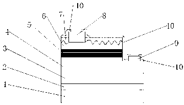
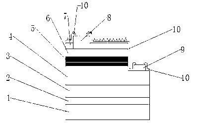
[0012] Refer to figure 1 , The present invention provides a method for manufacturing a GaN-based LED chip with a roughened surface, including the following steps:

[0013] Step 1: Using metal organic chemical vapor deposition (MOCVD) method, grow 20nmAlN, 2nm undoped GaN, 1nmGaN, 20nm current diffusion layer, (2nmInGaN+12.5nmGaN)*9MQW, 20nmP-GaN on semiconductor substrate 1 in sequence , Forming a GaN epitaxial wafer, wherein the semiconductor substrate 1 is sapphire, silicon, silicon carbide or metal;

[0014] Step 2: Put the GaN epitaxial wafer into PECVD, and quickly deposit silicon oxide or silicon nitride as a mask for etching on the surface of the P-GaN layer 6, or selectively deposit metals and other substances;

[0015] Step 3: Using the deposited nano-silicon oxide island as an etching mask, perform ICP (inductively coupled plasma) etching on the GaN epitaxial wafer, using Cl 2 , BCl 3 , Ar is used as an etching gas. After the etching is completed, the mask is removed with p...


PUM

PropertyMeasurementUnit
diameteraaaaaaaaaa
surface roughnessaaaaaaaaaa

Abstract

The invention discloses a manufacture method of a GaN (gallium nitride)-based LED (light emitting diode) chip with a roughened surface. The manufacture method comprises the steps that a metal organic chemical vapor deposition method is adopted, a low-temperature GaN buffer layer, an undoped GaN layer, a n-GaN layer, a multi-quantum well layer and a P-GaN layer are sequentially grown on a semiconductor substrate, and a GaN epitaxial wafer is formed; the GaN epitaxial wafer enters PECVD (plasma enhanced chemical vapor deposition) equipment so that sediments are in a nanometer island shape; the epitaxial wafer with the roughened surface is formed by using the nanometer island as an etching mask; one side of the GaN epitaxial wafer is subjected to etching, and a table surface is formed; an ITO (indium tin oxide) film is evaporated on the upper surface of the epitaxial wafer; and a P electrode is manufactured on P-GaN of the GaN epitaxial wafer, an N electrode is manufactured on n-GaN, and the device preparation is completed. The manufacture method has the advantages that the photoetching is not needed, the mask is automatically removed in the etching roughening process, the process is simple, the cost is low, the roughening effect is good, and the light extraction efficiency is high.

Description

Technical field [0001] The invention relates to the field of optoelectronic devices, in particular to a method for manufacturing a GaN-based LED chip with a roughened surface. Background technique [0002] There are two main factors in the luminous efficiency of light-emitting diodes (LEDs): the internal quantum effect and the external quantum effect of the device. At present, the internal quantum efficiency of a typical GaN blue LED can reach 80%. Therefore, it is unlikely that the internal quantum efficiency will be further improved significantly. Compared with the internal quantum efficiency, the external quantum efficiency of ordinary GaN-based LEDs is only a few percent. This is due to the large difference in refractive index between GaN and air. The critical angle of total reflection at the interface between GaN and air is 23 degrees. Only a small part of the light generated in the source area can be emitted into the air. In order to improve the light extraction efficienc...

Claims


Application Information

Patent Timeline
Patent Type & Authority Applications(China)
IPC IPC(8): H01L33/22H01L33/00
Inventor 宋超刘榕张建宝
Owner HC SEMITEK CORP
Why Eureka
Try Eureka