Sputtering target, compound semiconductor thin film, solar cell having compound semiconductor thin film, and method for manufacturing compound semiconductor thin film

A manufacturing method and sputtering target technology, which is applied in the field of sputtering targets, can solve problems such as high volume resistance, difficulty in making crystallinity, and easy breakdown, and achieve the effects of reducing volume resistance, suppressing abnormal discharge, and reducing redundant processes

Active Publication Date: 2012-10-03
JX NIPPON MINING & METALS CORP
View PDF15 Cites 6 Cited by
  • Summary
  • Abstract
  • Description
  • Claims
  • Application Information

AI Technical Summary

Problems solved by technology

[0006] Direct current (DC) sputtering with high film formation speed and excellent productivity can be performed using a CIGS alloy sintered body as a sputtering target. , there are the following problems: abnormal discharge such as breakdown is prone to occur, particles are generated in the film, and film quality deteriorates
[0009] However, in the methods described in Patent Document 1 to Patent Document 3, the supply of alkali metal from the alkali metal-containing layer to the CIGS layer is carried out by thermal diffusion during CuGa selenization, and it is difficult to accurately control the presence of alkali metal in the CIGS layer. Concentration distribution in
[0010] The reason for this is that when Na-containing soda-lime glass is used as a substrate, on the one hand, since the softening temperature is about 570°C, cracks are likely to occur at a high temperature of 600°C or higher, so it should not be too high. temperature, on the other hand, if selenization treatment is not performed at a high temperature of about 500°C or higher, it is difficult to fabricate a CIGS film with good crystallinity
That is, there is a problem that the controllable temperature range during selenization is very narrow, and it is difficult to control the proper diffusion of Na in the above temperature range.
However, as its production method, there is only a description of sintering the raw material powder synthesized independently by hot pressing, and the specific production method is not clarified.
In addition, there is no description of the oxygen concentration and volume resistance of the obtained sintered body.

Method used


Image

  • Sputtering target, compound semiconductor thin film, solar cell having compound semiconductor thin film, and method for manufacturing compound semiconductor thin film

Examples


Embodiment 1

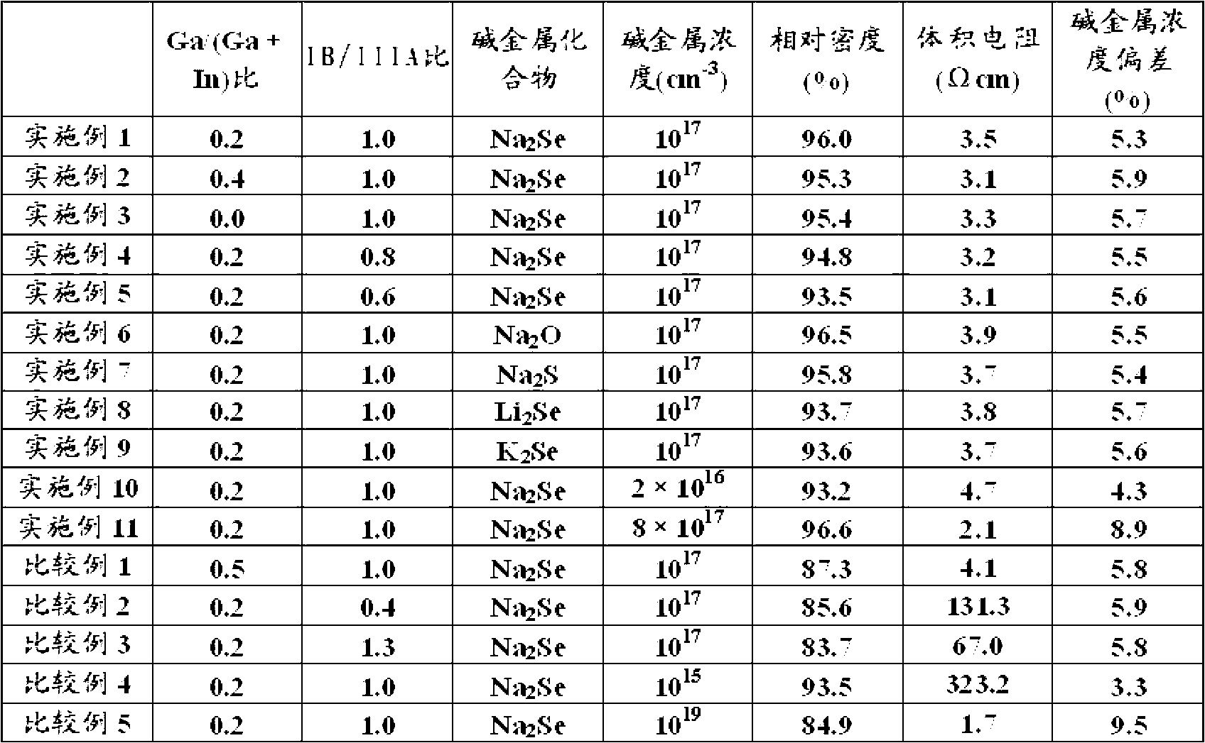
[0082] Weigh raw materials Cu, In, Ga, Se and Na 2 For Se, Ga / (Ga+In), which is the atomic ratio of Ga and In, is 0.2, and Cu / (Ga+In), which is the atomic ratio of Cu as a group IB element to the total of Ga and In as a group IIIA element, is 0.2. In) is 1.0, so that the concentration of Na is 10 17 cm -3 .

[0083] Next, these raw materials are put into a quartz ampoule, the inside is evacuated, sealed, and synthesized in a heating furnace. The heating program is set as follows: from room temperature to 100°C at a heating rate of 5°C / minute, then to 400°C at a heating rate of 1°C / minute, and then to 400°C at a heating rate of 5°C / minute Speed ​​is heated up to 550 DEG C, then, is heated up to 650 DEG C with the heating rate of 1.66 DEG C / min, then, keeps 8 hours at 650 DEG C, then, reaches room temperature after cooling in furnace with 12 hours.

[0084] The Na-added CIGS synthetic raw material powder obtained above was passed through a 120-mesh sieve, and then subjected ...

Embodiment 2~3

[0092] In embodiment 2, the atomic number ratio of Ga and In is set as Ga / (Ga+In)=0.4, and in embodiment 3, the atomic number ratio of Ga and In is set as Ga / (Ga+In)= 0.0, except that, under the same conditions as in Example 1, preparation of a sintered body and preparation of a thin film were performed. The results of the properties of the sintered body and the thin film are similarly shown in Table 1.

[0093] As shown in the above Table 1, in Example 2, the relative density is 95.3%, the volume resistance value is 3.1Ωcm, and the alkali concentration deviation is 5.9%. In Example 3, the relative density is 95.4%, and the volume resistance value is 3.3 Ωcm and the concentration variation of the alkali metal were 5.7%, both showing good values ​​for achieving the object of the present invention.

Embodiment 4~5

[0095] Cu / (Ga+In)=0.8 and Cu / (Ga+In)=0.6 respectively, except that Cu / (Ga+In)=0.6 are respectively set as Cu / (Ga+In)=0.6 with respect to the total atomic ratio of Cu which is a group IIIA element with respect to Ga and In which are a group IIIA element, Under the same conditions as in Example 1, production of a sintered body and production of a thin film were performed. The results of the properties of the sintered body and the thin film are similarly shown in Table 1.

[0096] As shown in the above table 1, in embodiment 4, the relative density is 94.8%, the volume resistance value is 3.2Ωcm, and the alkali concentration deviation is 5.5%, and in embodiment 5, the relative density is 93.5%, and the volume resistance value is 3.1 Ωcm and the concentration variation of the alkali metal were 5.6%, both showing good values ​​for achieving the object of the present invention.


PUM

PropertyMeasurementUnit
densityaaaaaaaaaa

Abstract

Disclosed is a sputtering target, which contains an alkali metal, is composed of an Ib element, IIIb element and VIb element, and has a chalcopyrite crystal structure. The sputtering target has the chalcopyrite crystal structure composed of a Ib-IIIb-VIb element, said structure being suitable for manufacturing, by sputtering one time, a light-absorbing layer having the chalcopyrite structure composed of the Ib-IIIb-VIb element.

Description

technical field [0001] The present invention relates to a sputtering target, particularly a sputtering target for producing a compound semiconductor thin film used as a light-absorbing layer of a thin-film solar cell, a method for producing the target, a compound semiconductor thin film formed using the sputtering target, and the sputtering target. A solar cell having a compound semiconductor thin film as a light absorbing layer and a method for manufacturing the compound semiconductor thin film. Background technique [0002] In recent years, mass production of high-efficiency Cu—In—Ga—Se (hereinafter referred to as CIGS) solar cells has been advanced as thin film solar cells. A vapor deposition method and a selenization method are known as methods for producing the CIGS layer which is the light-absorbing layer. [0003] Solar cells manufactured by vapor deposition have the advantage of high conversion efficiency, but have disadvantages such as low film formation speed, hig...

Claims


Application Information

Patent Timeline
Patent Type & Authority Applications(China)
IPC IPC(8): C23C14/34H01L31/04
CPCH01L31/0322C23C14/0629C23C14/0623C23C14/3414Y02E10/541Y02P70/50
Inventor 生泽正克高见英生田村友哉
Owner JX NIPPON MINING & METALS CORP
Why Eureka
Try Eureka