A kind of soi BJT dual-strain plane BiCMOS integrated device and its preparation method

An integrated device and double-strain technology, which is applied in semiconductor/solid-state device manufacturing, electric solid-state devices, semiconductor devices, etc., can solve the problems of low mechanical strength, complex preparation process compared with Si process, and incompatibility

Inactive Publication Date: 2015-08-12
XIDIAN UNIV
View PDF4 Cites 0 Cited by
  • Summary
  • Abstract
  • Description
  • Claims
  • Application Information

AI Technical Summary

Problems solved by technology

[0007] In order to improve the performance of devices and integrated circuits, researchers use new semiconductor materials such as GaAs, InP, etc. to obtain high-speed devices and integrated circuits suitable for the development of wireless mobile communications; although GaAs and InP-based compound devices have superior frequency characteristics, but Its preparation process is more complicated than the Si process, the cost is high, the preparation of large-diameter single crystal is difficult, the mechanical strength is low, the heat dissipation performance is not good, it is difficult to be compatible with the Si process, and it lacks SiO 2 Such passivation layer and other factors limit its wide application and development.

Method used


Image

  • A kind of soi BJT dual-strain plane BiCMOS integrated device and its preparation method

Examples


Embodiment 1

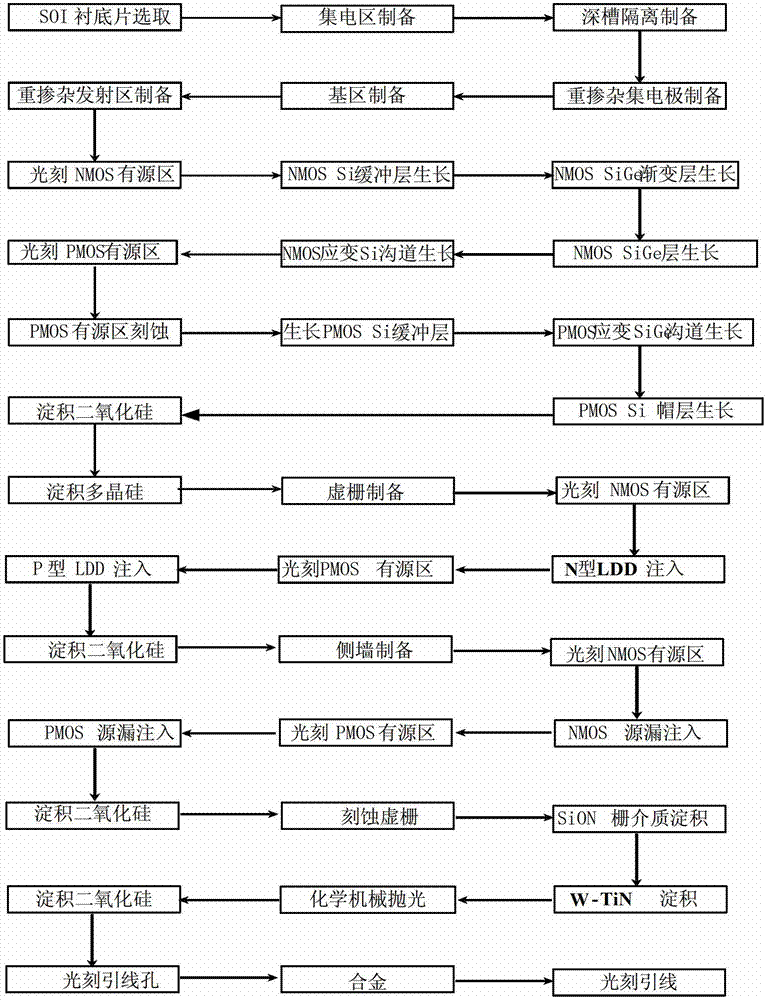
[0096] Embodiment 1: Prepare SOI BJT, dual strain plane BiCMOS integrated device and circuit with conductive channel of 45nm, the specific steps are as follows:

[0097] Step 1, epitaxial growth.

[0098] (1a) Select the SOI substrate, the support material of the lower layer of the substrate is Si, and the middle layer is SiO 2 , with a thickness of 150nm, and the upper material is doped with a concentration of 1×10 16 cm -3 N-type Si with a thickness of 100nm;

[0099] (1b) Thermally oxidize a layer of SiO with a thickness of 300nm on the substrate surface 2 layer.

[0100] Step 2, isolation area preparation.

[0101] (2a) Epitaxially grow a layer with a doping concentration of 1×10 on the SOI substrate 16 cm -3 The Si layer, with a thickness of 200nm, serves as the collector area;

[0102] (2b) Thermally oxidize a layer of SiO with a thickness of 300nm on the substrate surface 2 layer;

[0103] (2c) In the photolithographic isolation area, a deep trench with a dept...

Embodiment 2

[0145] Embodiment 2: The preparation of SOI BJT with a conductive channel of 30nm, double strained plane BiCMOS integrated devices and circuits, the specific steps are as follows:

[0146] Step 1, epitaxial growth.

[0147] (1a) Select the SOI substrate, the support material of the lower layer of the substrate is Si, and the middle layer is SiO 2 , with a thickness of 300nm, and the upper material is doped with a concentration of 5×10 16 cm -3 N-type Si with a thickness of 120nm;

[0148] (1b) Thermally oxidize a layer of SiO with a thickness of 400nm on the substrate surface 2 layer.

[0149] Step 2, isolation area preparation.

[0150] (2a) Epitaxially grow a layer with a doping concentration of 5×10 on the SOI substrate 16 cm -3 The Si layer, with a thickness of 350nm, serves as the collector area;

[0151] (2b) Thermally oxidize a layer of SiO with a thickness of 400nm on the surface of the substrate 2 layer;

[0152] (2c) In the photolithographic isolation area,...

Embodiment 3

[0194] Embodiment 3: prepare SOI BJT, dual strain plane BiCMOS integrated device and circuit with conductive channel of 22nm, the specific steps are as follows:

[0195] Step 1, epitaxial growth.

[0196] (1a) Select the SOI substrate, the support material of the lower layer of the substrate is Si, and the middle layer is SiO 2 , with a thickness of 400nm, and the upper material is doped with a concentration of 1×10 17 cm -3 N-type Si with a thickness of 150nm;

[0197] (1b) Thermally oxidize a layer of SiO with a thickness of 500nm on the surface of the substrate 2 layer.

[0198] Step 2, isolation area preparation.

[0199] (2a) Epitaxially grow a layer with a doping concentration of 1×10 on the SOI substrate 17 cm -3 The Si layer, with a thickness of 400nm, serves as the collector area;

[0200] (2b) Thermally oxidize a layer of SiO with a thickness of 500nm on the substrate surface 2 layer;

[0201] (2c) In the photolithographic isolation area, a deep trench with...


PUM


Abstract

The invention discloses an SOI (Silicon-On-Insulator)-BJT (Bipolar Junction Transistor) double-strain-plane Bi CMOS (Complementary Metal-Oxide-Semiconductor) integrated device and a preparation method of the device. The preparation process is as follows: growing an N type Si epitaxial collector region on an SOI substrate sheet, preparing a deep-trench isolator, and manufacturing a conventional Si bipolar transistor in a bipolar device region; etching a deep trench in an active region of an MOS (Metal Oxide Semiconductor) device by utilizing a dry etching process, and respectively and selectively growing a P type Si layer, a P type SiGe gradual change layer, a P type SiGe layer, a P type strain Si layer which are taken as an active region of an NMOS (N-Channel Metal Oxide Semiconductor) device, an N type Si layer, an N type strain SiGe layer and an N type Si cap layer which are taken as an active region of a PMOS (P-Channel Metal Oxide Semiconductor) device in the trench in an epitaxial manner; and preparing a virtual grid electrode, respectively injecting LDD (Laser Detector Diode) of the MOS device, depositing SiO2, preparing a side wall, and conducting self alignment to form source drain of the NMOS device and the PMOS device; and etching a virtual grid, depositing a SiON grid dielectric layer and a W-TiN composite grid, and thus finally forming the Bi CMOS integrated device with the channel being 22-45nm. According to the method, the tensile strain Si with high electronic mobility and compressive strain SiGe with high hole mobility are respectively taken as conducting channels of the NMOS device and the PMOS device, so that the performances of the Bi CMOS integrated device and a circuit are improved greatly.

Description

technical field [0001] The invention belongs to the technical field of semiconductor integrated circuits, and in particular relates to an SOI BJT and double strain plane BiCMOS integrated device and a preparation method. Background technique [0002] The integrated circuit, which appeared in 1958, is one of the most influential inventions of the 20th century. Microelectronics based on this invention has become the basis of existing modern technology, accelerating the process of knowledge and informationization of human society, and at the same time changing the way of thinking of human beings; it not only provides human beings with powerful It is not only a tool for transforming nature, but also opens up a broad space for development. [0003] Semiconductor integrated circuits have become the basis of the electronics industry. People's huge demand for the electronics industry has prompted the rapid development of this field; in the past few decades, the rapid development of...

Claims


Application Information

Patent Timeline
Patent Type & Authority Patents(China)
IPC IPC(8): H01L27/12H01L21/84
Inventor 胡辉勇宋建军宣荣喜张鹤鸣王海栋舒斌王斌郝跃
Owner XIDIAN UNIV
Why Eureka
Try Eureka