

Method for manufacturing three-dimensional superconduction micro-nano device
A superconducting and device technology, applied in the direction of nanotechnology, nanotechnology, nanostructure manufacturing, etc., can solve problems such as parasitic effects and noise, affecting the actual performance of devices, etc., and achieve the effect of improving efficiency and high process controllability
- Summary
- Abstract
- Description
- Claims
- Application Information
AI Technical Summary
Problems solved by technology
Method used
Image

Examples
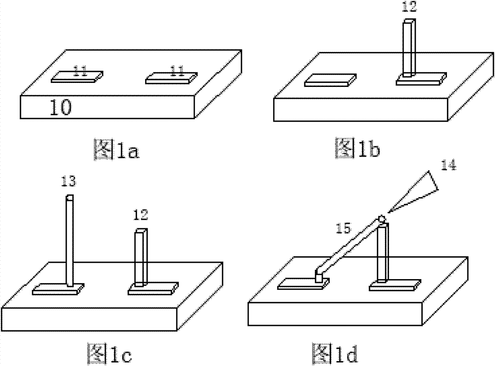
Embodiment 1
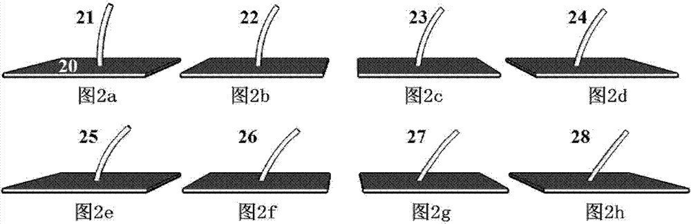
[0088] SiO based on focused ion beam material growth and irradiation 2 The three-dimensional deformation control of superconducting tungsten nanowires on a / Si substrate includes the following steps:
[0089] (1) Sample placement and fixation:
[0090] SiO 2 / Si substrate (20) is fixed on a sample holder with a horizontal surface from the back of the substrate with conductive carbon tape, and the sample fixed on the sample holder is placed on the sample stage in the double beam SEM / FIB cavity. The system used The angle between the incident direction of FIB and the horizontal plane is 38°.
[0091] (2) Growth of superconducting tungsten nanowires perpendicular to the substrate
[0092] Evacuate, after the vacuum meets the requirements, turn on the electron gun (5kV electron beam acceleration voltage, 30μm electron beam diaphragm) and ion gun (30kV ion beam acceleration voltage, 1pA ion beam current), and tilt the sample stage 52° to make The ion beam is incident perpendicular to the su...
Embodiment 2
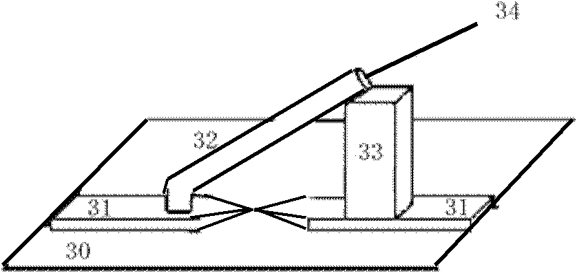
[0108] SiO 2 The preparation of a tungsten three-dimensional superconducting detection coil perpendicular to the superconducting quantum interference device in the plane of the / Si substrate includes the following steps:
[0109] 1) Preparation of superconducting Josephson junction devices: in SiO 2 / Si substrate (30) adopts plasma laser deposition to grow Nb film, and then forms the resist pattern of Josephson junction device by photolithography, and then adopts reactive ion dry etching-deglue to obtain image 3 The device structure shown in 31.
[0110] 2) Growth of tungsten nano-piers: Fix the sample obtained in 1) on the sample holder with conductive silver glue, send it into the SEM / FIB cavity and fix it on the sample stage; tilt the sample stage clockwise by 52° to make the lining The bottom surface is perpendicular to the incident direction of the ion beam. Tungsten source for heating GIS (W(CO) 6 ), turn on the electron beam ion beam, select the ion beam current of 10pA, a...
PUM
 Abstract
Description
Claims
Application Information