

SiC vertical double diffusion metal oxide semiconductor structure (VDMOS) device with composite gate dielectric structure
A technology of compound gate dielectric and gate dielectric, used in semiconductor devices, electrical components, circuits, etc., can solve problems such as reducing channel mobility, avoid premature breakdown, good surface quality, and weaken the reduction of breakdown voltage. Effect
- Summary
- Abstract
- Description
- Claims
- Application Information
AI Technical Summary
Problems solved by technology
Method used
Image

Examples
Embodiment Construction
[0017] In order to make the technical solution to be explained in the present invention and the superiority of the present invention clearer, the specific implementation manners of the present invention will be described in detail below in conjunction with the accompanying drawings. The specific embodiments described here are only used to explain the present invention, not to limit the present invention.
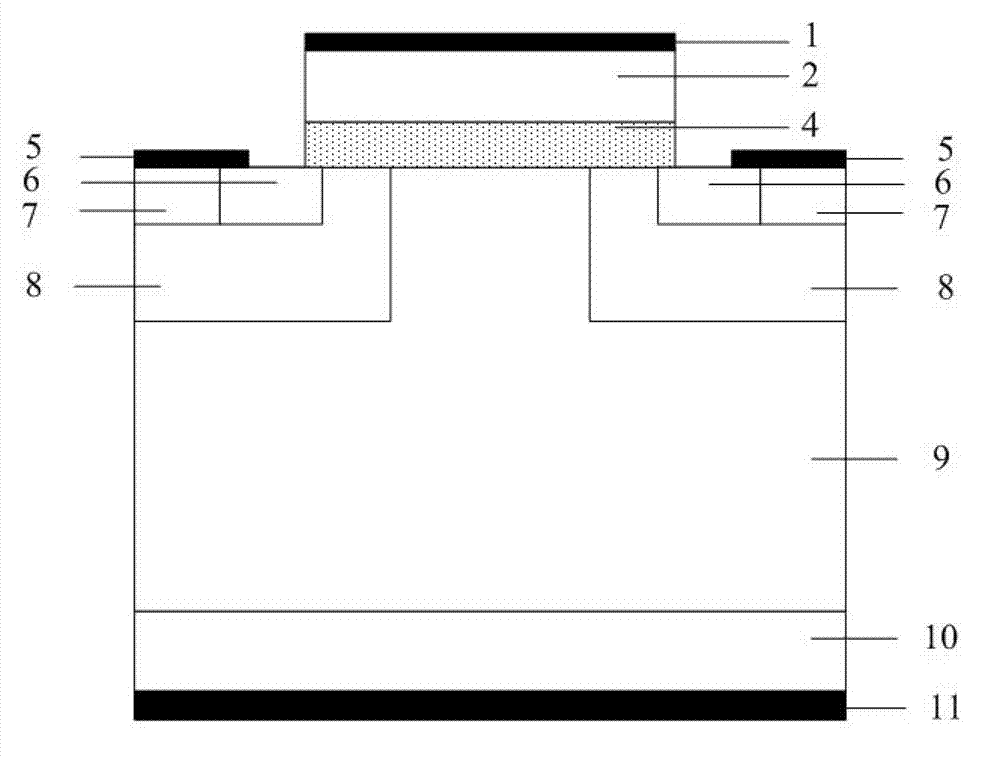
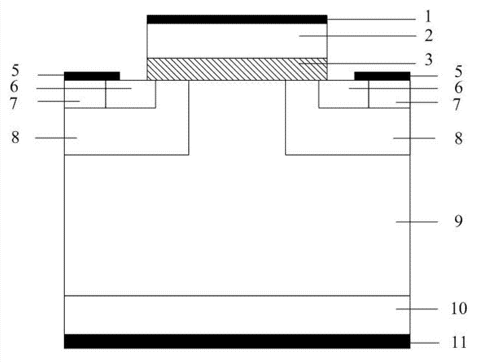
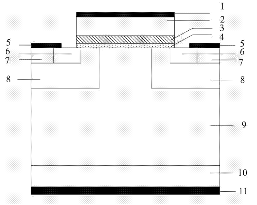
[0018] A SiC VDMOS device with a compound gate dielectric structure, its cell structure is as follows Figure 4 As shown, it includes: metal gate electrode 1, polysilicon gate 2, gate dielectric, metal source electrode 5, silicon carbide N + Source region 6, silicon carbide P + Contact area 7, SiC P-base area 8, SiC Nˉdrift area 9, SiC N + Substrate 10, metal drain electrode 11; cells from bottom to top are metal drain electrode 11, silicon carbide N + Substrate 10, silicon carbide N – Drift region 9; there is a silicon carbide P-base region 8 on both sides of the top of...
PUM
 Abstract
Description
Claims
Application Information