

Three-family nitride-based phototransistor detector and manufacturing method thereof
A technology of phototransistor and manufacturing method, which is applied in the direction of semiconductor devices, electrical components, circuits, etc., can solve the influence of device light absorption efficiency and photogenerated carrier generation efficiency, and the p-type base memory effect has not been solved, which is not conducive to photogenerated carriers Problems such as carrier transport, to achieve the effect of improving photoelectric conversion efficiency, improving steepness, and reducing dark current
- Summary
- Abstract
- Description
- Claims
- Application Information
AI Technical Summary
Problems solved by technology
Method used
Image

Examples
Embodiment 1
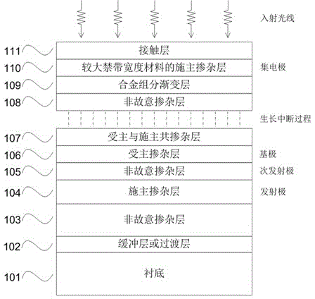
[0030] The structure of the III-nitride based phototransistor is as follows figure 1 Shown: substrate 101, buffer layer or transition layer 102, unintentionally doped layer 103, donor doped layer 104, unintentionally doped layer 105, acceptor doped layer 106, acceptor and donor co-doped layer 107 , an unintentionally doped layer 108 , a graded alloy composition layer 109 , a donor doped layer 110 of a material with a larger forbidden band width, and a contact layer 111 . The phototransistor is n-i-p-i-n type, the collector is on the top, the emitter is on the bottom, the base is in the middle, and the way of normal incidence is adopted. There are twelve steps to achieve this structure:
[0031] (1). The substrate 101 is placed in the reaction chamber, and the above-mentioned epitaxial structure is sequentially grown on the substrate by an epitaxial growth method. Epitaxial growth methods can use methods such as metal organic chemical vapor deposition (MOCVD), molecular beam ...
Embodiment 2
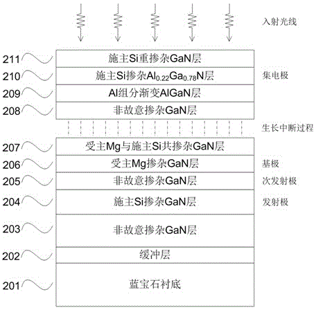
[0044] This example will specifically illustrate figure 1 The structure of the III-nitride-based phototransistor is shown, the phototransistor structure is n-i-p-i-n type, and adopts the form of normal incidence.
[0045] Such as figure 2 As shown, using the metal organic chemical vapor deposition (MOCVD) epitaxial growth method, a buffer layer 202, an unintentionally doped GaN layer 203, a donor Si-doped GaN layer 204, an unintentionally doped GaN layer 204, and an unintentionally doped Doped GaN layer 205, acceptor Mg doped GaN layer 206, acceptor Mg and donor Si co-doped GaN layer 207, unintentionally doped GaN layer 208, Al composition gradient AlGaN layer 209, donor Si doped Al 0.22 Ga 0.78 N layer 210 and donor Si heavily doped GaN layer 211 . According to the structure of the III-nitride-based phototransistor, it can be divided into ten functional structures, each of which will be described below.
[0046] (1). A buffer layer 202 and an unintentionally doped GaN la...
PUM
 Abstract
Description
Claims
Application Information