optical receiver

A technology of optical receivers and photodetectors, applied in the field of optoelectronics, can solve the problems of increasing the delay time of the input to the AGC circuit and system noise, the inability to respond to the rapid change of the burst mode signal level, and the longer AGC delay time, etc., to achieve Low input noise, high speed, and reduced settling time

Inactive Publication Date: 2015-09-16
UNIV OF ELECTRONICS SCI & TECH OF CHINA
View PDF7 Cites 0 Cited by
  • Summary
  • Abstract
  • Description
  • Claims
  • Application Information

AI Technical Summary

Problems solved by technology

Generally speaking, the preamplifier should have a higher transimpedance gain to avoid the decrease of the signal-to-noise ratio due to the influence of the noise of the main amplifier connected afterwards. This requires that the value of the resistor R1 connected to the output of the TIA should not be too small, otherwise The closed-loop gain will drop significantly at medium and high frequencies; also, the value of capacitor C1 should not be too small in order to obtain good filter characteristics, which results in a larger product of resistor R1 and capacitor C1, namely a larger time constant, and longer AGC delay time, unable to respond to sudden changes. Rapid changes in signal level in transmit mode
In addition, in order to obtain good open-loop characteristics, the TIA structure generally adopts a multi-stage circuit cascading method, which also increases the delay time and system noise input to the AGC circuit, and it is impossible to sacrifice the performance of the TIA in exchange for AGC in practice. fast response time

Method used


Image

  • optical receiver
  • optical receiver
  • optical receiver

Examples


Embodiment Construction

[0025] The present invention will be further described below in conjunction with the accompanying drawings and specific embodiments.

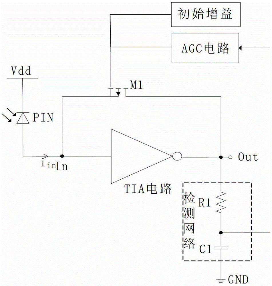
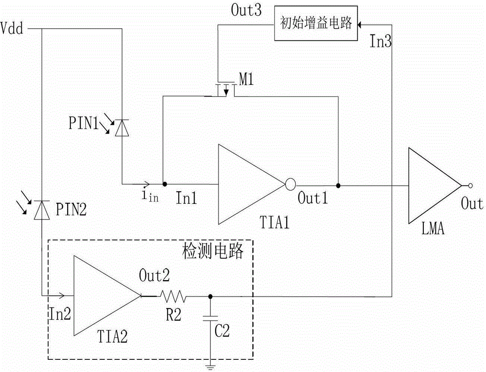
[0026] In the optical receiver, AGC is actually a circuit structure that quickly adjusts the output voltage according to the detected input current amplitude. The output voltage here is used to drive the NMOS gate in the deep linear region to change its equivalent resistance. . The general AGC circuit obtains the DC level of the circuit as its input signal from the output terminal of the TIA through the detection circuit. However, since the resistor replaced by the NMOS is actually more sensitive to the gate-source voltage, it does not require high gain and high input photogenerated current. Signal, so the DC level directly obtained from the output terminal needs to be processed by the amplifier before it can be added to the gate of the NMOS. The role of the AGC circuit is exactly the process of acquiring, processing, and converting the DC leve...


PUM


Abstract

The invention discloses an optical receiver which particularly comprises a first PIN-type photoelectric detector, a second PIN-type photoelectric detector, a first trans-impedance amplifier, a second trans-impedance amplifier, a resistance device, a capacitance device, a MOSFET (Metal Oxide Semiconductor Field Effect Transistor), an initial gain circuit and a limiting amplifier, wherein a detection circuit is formed by the second trans-impedance amplifier, the resistance device and the capacitance device; an automatic gain control circuit is formed by the second PIN-type photoelectric detector, the detection circuit and the initial gain circuit; and by introducing the second photoelectric detector and the second trans-impedance amplifier, the limitation on part of performance indexes of an original gain control circuit and an original trans-impedance amplifier circuit is effectively relieved, the stabilization time of AGC (Automatic Gain Control) is reduced and the noise input into the AGC circuit is reduced, so that the control accuracy is improved.

Description

technical field [0001] The invention belongs to the technical field of optoelectronics, and in particular relates to the design of an optical receiver. technical background [0002] Optical fiber communication is an important application of optoelectronic technology in the field of communication. The emergence and development of optical fiber communication has far-reaching significance in the history of communication development and is considered to be a fundamental change in the history of communication. The optical receiver is an indispensable and important part of the optical fiber communication system. Its function is to convert the weak optical signal output from the optical fiber line and generate distortion into an electrical signal, and generate an electrical signal for subsequent circuits after amplification and processing. . The optical receiver consists of a semiconductor photodetector (such as a PIN photodiode or MSM-PD diode) coupled with an optical fiber, a pr...

Claims


Application Information

Patent Timeline
Patent Type & Authority Patents(China)
IPC IPC(8): H04B10/61H04B10/66
Inventor 张有润吴浩然刘影张波
Owner UNIV OF ELECTRONICS SCI & TECH OF CHINA
Why Eureka
Try Eureka