

Method for improving luminous efficiency of AlGaN-based ultraviolet LED (Light-Emitting Diode)
A technology of luminous efficiency and high temperature, applied in electrical components, circuits, semiconductor devices, etc., can solve the problems of increased difficulty, easy wear and tear of thin films, and high production costs, to reduce stress and dislocation density, and not easy to wear and fall off. , simple in design and craftsmanship
- Summary
- Abstract
- Description
- Claims
- Application Information
AI Technical Summary
Problems solved by technology
Method used
Image

Examples
Embodiment 1
[0055] A method for improving the luminous efficiency of an AlGaN-based ultraviolet LED by using a double-sided patterned sapphire substrate, the operation is as follows:
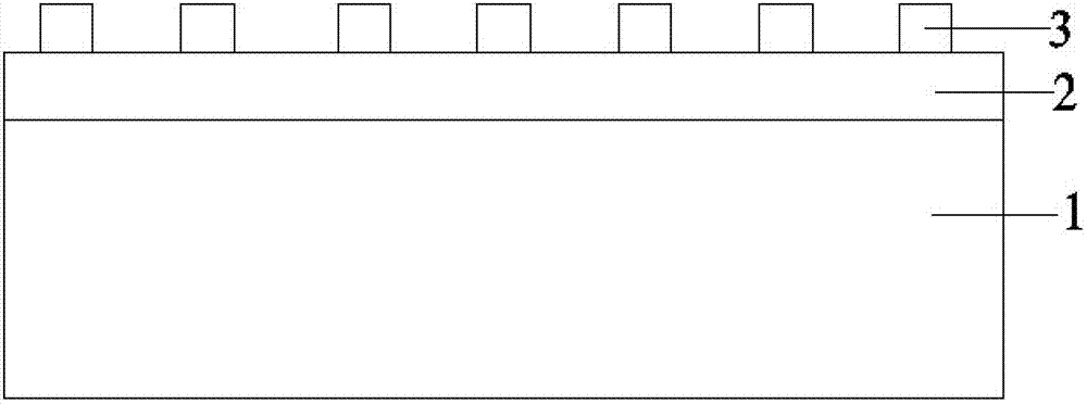
[0056] First, a 200nm silicon dioxide film 2 is deposited on a 2-inch c-plane sapphire substrate 1 using chemical vapor deposition (CVD) technology, and then a periodic photoresist pattern display 3 is made using conventional photolithography technology, and the pattern unit is rectangular , the spacing is 500nm, the cross-sectional view after photolithography is as follows figure 1 shown;
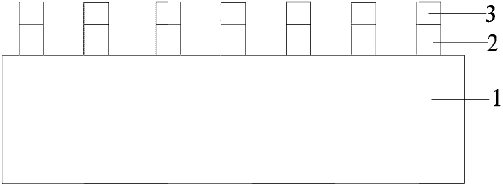
[0057] Next, using the photoresist pattern array as a mask, using a mixture of hydrofluoric acid and ammonium fluoride solution (mixing volume ratio is 1:7), etch a silicon dioxide film 2 with a pattern structure (such as figure 2 shown);
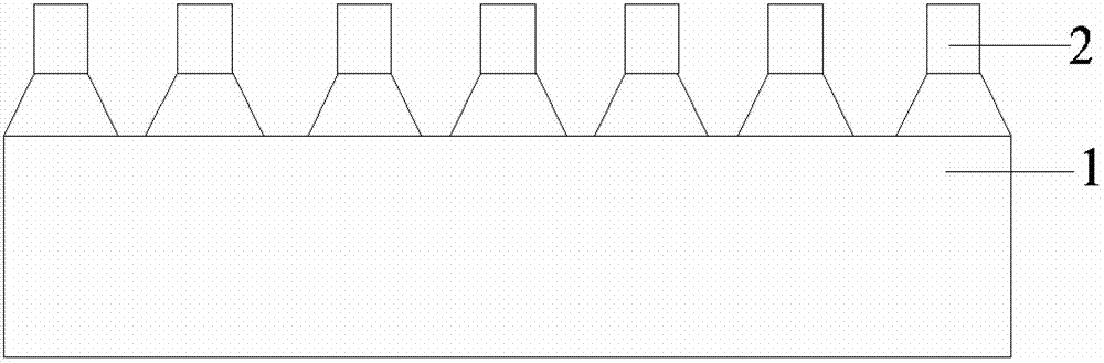
[0058] Then, using the silicon dioxide film 2 with a pattern structure as a mask plate, the c-plane sapphire substrate 1 is etched at 450°C for 10 minutes with a mixture of sulfur...
Embodiment 2
[0065] A method for improving the luminous efficiency of an AlGaN-based ultraviolet LED by using a double-sided patterned sapphire substrate, the operation is as follows:
[0066] First, a 1.0-micron silicon dioxide film 2 is deposited on a 2-inch c-plane sapphire substrate 1 using chemical vapor deposition (CVD) technology, and then a periodic photoresist pattern display 3 is made using conventional photolithography technology. The pattern unit is Rectangular, with a pitch of 1.0 microns, the cross-sectional view after photolithography is as follows figure 1 shown;
[0067] Next, using the photoresist pattern array as a mask, using a mixture of hydrofluoric acid and ammonium fluoride solution (mixing volume ratio is 1:7), etch a silicon dioxide film 2 with a pattern structure (such as figure 2 shown);
[0068] Then, using the silicon dioxide film 2 with a pattern structure as a mask plate, the c-plane sapphire substrate 1 is etched at 450°C for 10 minutes with a mixture of...
PUM
 Abstract
Description
Claims
Application Information