
Transition layer for CIGS-based film photovoltaic cell and preparation method of transition layer

A thin-film photovoltaic cell and transition layer technology, which is used in circuits, electrical components, and final product manufacturing, etc., can solve the problems that the metal molybdenum electrode layer and the glass substrate are not firmly combined, and achieve the problem of poor adhesion, good transition connection, Combines a strong effect

Active Publication Date: 2013-01-09
厦门神科太阳能有限公司
View PDF5 Cites 4 Cited by
  • Summary
  • Abstract
  • Description
  • Claims
  • Application Information

AI Technical Summary

Problems solved by technology

[0007] Another object of the present invention is to solve the problems in the prior art: the problem that the bonding between the metal molybdenum electrode layer and the glass substrate is not strong enough

Method used

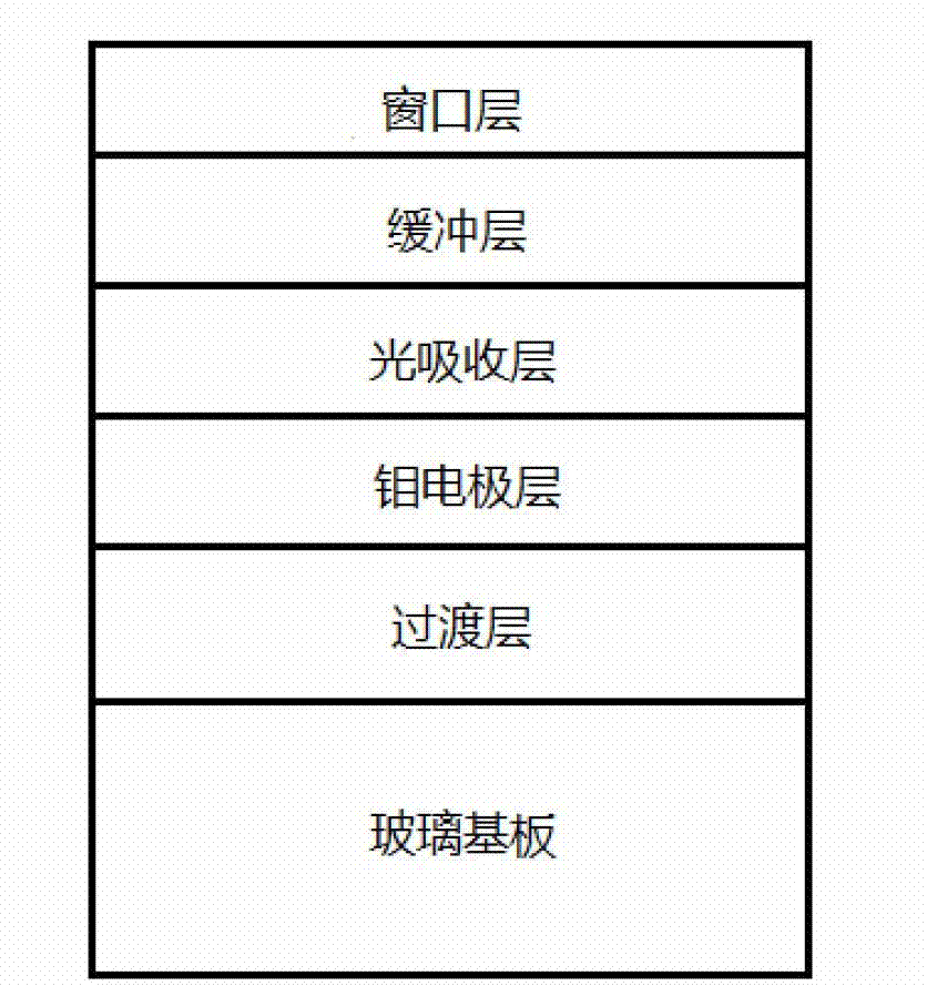
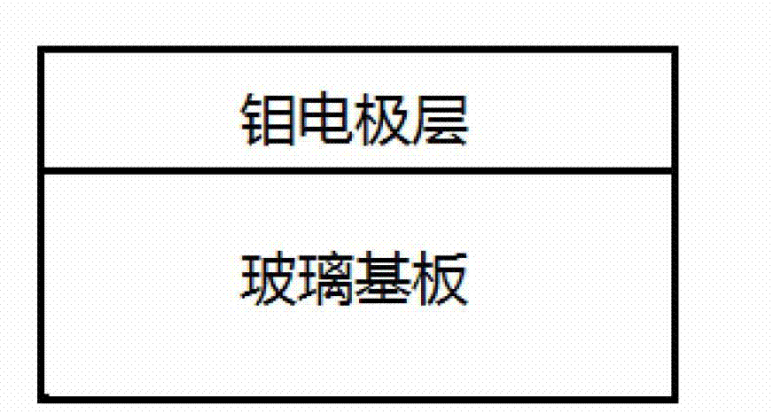

Image

  • Transition layer for CIGS-based film photovoltaic cell and preparation method of transition layer
  • Transition layer for CIGS-based film photovoltaic cell and preparation method of transition layer
  • Transition layer for CIGS-based film photovoltaic cell and preparation method of transition layer

Examples


Embodiment 1

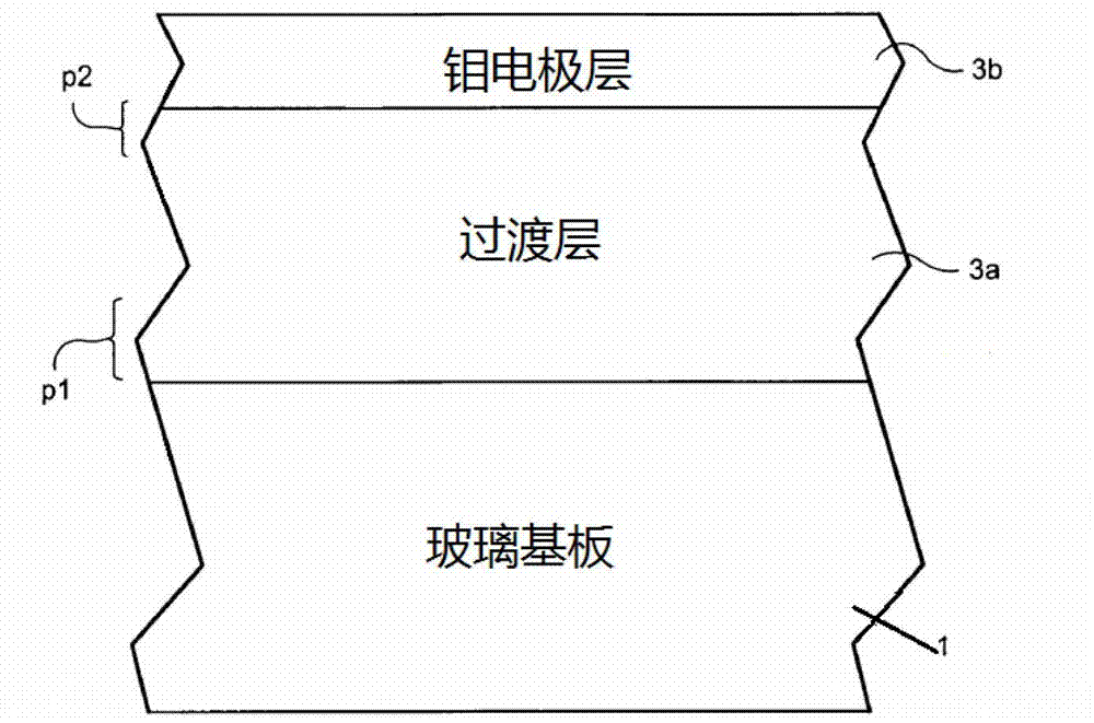
[0037] A transition layer 3 a with a thickness of 15 nm and a molybdenum electrode layer with a thickness of 400 nm are sequentially deposited on a soda lime glass substrate with a thickness of 3.0 mm. Both the transition layer 3a and the molybdenum electrode layer are deposited by magnetron sputtering, and the deposition of the transition layer 3a uses three kinds of targets: an alloy target containing 25% silicon, 70% zirconium, and 5% molybdenum is the first sputtering target. The target, the alloy target containing 35% silicon, 30% zirconium, and 35% molybdenum is the second sputtering target, and the alloy target containing 10% silicon, 5% zirconium, and 85% molybdenum is the third sputtering target. The soda-lime glass substrate is sequentially passed under the first sputtering target, the second sputtering target and the third sputtering target, and argon and oxygen are introduced during the sputtering deposition process to form each layer with a thickness of about 5 nm....

Embodiment 2

[0041] A transition layer 3 a with a thickness of 15 nm and a molybdenum electrode layer with a thickness of 400 nm are sequentially deposited on a soda lime glass substrate with a thickness of 3.0 mm. Both the transition layer 3a and the molybdenum electrode layer are deposited by magnetron sputtering, and the deposition of the transition layer 3a uses three targets: an alloy target containing 20% ​​silicon, 70% zirconium, and 10% titanium is the first sputtering The target, the alloy target containing 35% silicon, 30% zirconium and 35% molybdenum is the second sputtering target, and the target containing 100% molybdenum is the third sputtering target. The soda-lime glass substrate is sequentially passed under the first sputtering target, the second sputtering target and the third sputtering target, and argon and nitrogen are introduced during the sputtering deposition process to form each layer with a thickness of about 5 nm. Transition layer 3a with a thickness of 15 nm. T...

Embodiment 3

[0045] A transition layer 3 a with a thickness of 15 nm and a molybdenum electrode layer with a thickness of 400 nm are sequentially deposited on a soda lime glass substrate with a thickness of 3.0 mm. Both the transition layer 3a and the molybdenum electrode layer were deposited by magnetron sputtering, and the transition layer 3a was deposited using an alloy target containing 15% silicon, 60% zirconium, and 25% molybdenum. The soda-lime glass substrate is passed under the sputtering target, and argon, oxygen and nitrogen are introduced during the sputtering deposition process to form a transition layer 3 a with a thickness of 15 nm. Thus obtained with figure 2 The transition layer of the structure shown.

[0046] Laminate coated glass, 0.76mm PVB and another 3.0mm original glass sheet to make laminated glass. Do a knock test on the laminated glass, and the level of the knock test is 3, which shows that the adhesion of the film layer to the glass substrate and PVB is very ...


PUM


Abstract

The invention discloses a transition layer for a CIGS-based film photovoltaic cell and a preparation method of the transition layer. The preparation method comprises the steps of: providing a soda-lime glass substrate, forming a transition layer covering the surface of the soda-lime glass substrate, forming a molybdenum layer covering the transition layer, forming a light absorbing layer having a copper pyrite structure and covering the molybdenum layer, forming a buffer layer covering the light absorbing layer, and forming a window layer covering the buffer layer. According to the invention, the transition layer is deposited on the surface of the glass substrate, thus the adhesion problem between a molybdenum electrode layer and the glass substrate can be efficiently solved, and sodium materials can be prevented from uncontrollably diffusing into the light absorbing layer.

Description

technical field [0001] The invention relates to the technical field of thin film solar cells, in particular to a transition layer of a copper indium gallium selenide (sulfur) thin film cell with a chalcopyrite structure and a preparation method thereof. Background technique [0002] With the global warming, the deterioration of the ecological environment and the shortage of conventional energy, more and more countries have begun to vigorously develop solar energy utilization technology. Solar photovoltaic power generation is a zero-emission clean energy, which has the advantages of safety, reliability, no noise, no pollution, inexhaustible resources, short construction period, and long service life, so it has attracted much attention. Copper indium gallium selenide (CIGS) is a direct bandgap P-type semiconductor material with an absorption coefficient as high as 10 5 / cm, 2um thick copper indium gallium selenide film can absorb more than 90% of sunlight. The band gap of th...

Claims


Application Information

Patent Timeline
Patent Type & Authority Applications(China)
IPC IPC(8): H01L31/0352H01L31/18
CPCY02P70/50
Inventor 李艺明田宏波
Owner 厦门神科太阳能有限公司
Learn More