
Method for manufacturing conducting circuit by additive process

A conductive circuit and process technology, which is applied in the field of conductive circuit preparation by additive process, can solve the problems of the conductivity of nano-copper ink conductive copper paste is not very ideal, which limits the large-scale application of printed electronic technology, and achieves excellent adhesion , Reduce the cost of equipment improvement, the effect of short production cycle

Inactive Publication Date: 2013-01-16
FUDAN UNIV
View PDF5 Cites 11 Cited by
  • Summary
  • Abstract
  • Description
  • Claims
  • Application Information

AI Technical Summary

Problems solved by technology

The use of silver as a conductive unit has the advantages of high conductivity and stable properties, but the high price of silver also limits the large-scale application of printed electronic technology
Replacing silver with copper can solve the cost problem, but the fine particles of copper are easily oxidized by air, resulting in poor conductivity of both nano-copper ink and conductive copper paste

Method used


Image

  • Method for manufacturing conducting circuit by additive process

Examples


Embodiment 1

[0033] (1) Take 10g of polyurethane resin, add 5g of nano-calcium carbonate, 0.5g of γ-mercaptopropyltrimethoxysilane, 0.6g of methyltrimethoxysilane, 0.3g of γ-glycidyl etheroxypropyltrimethoxysilane, 10g mixed solvent (0.5g water, 0.2g methanol, 0.3g ethanol, 0.1g acetylacetone, 0.1g acetone, 7.5g butyl acetate, 0.5g ethylene glycol methyl ether, 0.8g ethylene glycol butyl ether), 0.1g Polyvinylpyrrolidone is mixed and stirred at 500 rpm for 24 hours, and the measured viscosity is greater than 6000 centipoise, and the preparation of the film-forming agent is completed;

[0034] (2) Use polyimide as the substrate, soak the substrate in 1mol / L sodium hydroxide solution for 10 minutes before use, and then clean it with deionized water;

[0035] (3) Use a 500-mesh screen film-forming agent to print circuit patterns on the substrate;

[0036] (4) Heat the printed circuit at 80oC for 1 hour;

[0037] (5) Immerse the treated substrate in 0.1mol / L palladium chloride solution for 1...

Embodiment 2

[0046](1) Take 5g of diethylenetriaminopropyltrimethoxysilane, 5g of methyltrimethoxysilane, 15g of mixed solvent (3g of water, 2g of methanol, 1g of ethanol, 1g of acetylacetone, 1g of ethylene glycol methyl ether, ethyl Glycol butyl ether 2g isopropanol 3.5g, acetone 1.5g), mixing and stirring at 500 rpm / min for 24 hours, the measured viscosity is less than 100 centipoise, and the film-forming agent is prepared;

[0047] (2) Use polyethylene terephthalate as the substrate, soak the substrate in 1mol / L sodium hydroxide solution for 10 minutes before use, and then clean it with deionized water;

[0048] (3) Use a 50um nozzle inkjet printer to print out circuit graphics;

[0049] (4) Heat the printed circuit at 70oC for 1 hour;

[0050] (5) Immerse the treated substrate in 0.1mol / L silver nitrate solution for 1 hour;

[0051] (6) Wash off excess catalyst by soaking in deionized water;

[0052] (7) Dry at 50oC for 10 minutes;

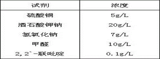
[0053] (8) Configure electroless copper plating...

Embodiment 3

[0059] (1) Take 5g of 3-aminopropyltrimethoxysilane, 3g of dimethyldimethoxysilane, 2g of phenyltrimethoxysilane, 15g of mixed solvent (3g of water, 2g of methanol, 1g of ethanol, 1g of acetylacetone, ethyl Glycol methyl ether 1g, ethylene glycol butyl ether 2g isopropanol 3.5g, acetone 1.5g), mixed and stirred at 500 rpm / min for 24 hours, the measured viscosity was less than 100 centipoise, and the film-forming agent was prepared;

[0060] (2) Use polyethylene terephthalate as the substrate, soak the substrate in 1mol / L sodium hydroxide solution for 10 minutes before use, and then clean it with deionized water;

[0061] (3) Use a 50um nozzle inkjet printer to print out circuit graphics;

[0062] (4) heat-treat the printed circuit at 70oC for 1 hour;

[0063] (5) Immerse the treated substrate in 0.1mol / L silver nitrate solution for 1 hour;

[0064] (6) Soak and wash off excess catalyst with deionized water;

[0065] (7) Dry at 50oC for 10 minutes;

[0066] (8) Configure th...


PUM


Abstract

The invention belongs to the field of manufacture of printed circuit boards, and particularly discloses a method for manufacturing a conducting circuit by an additive process. The method particularly includes steps of adding fillers, solvents and auxiliaries in epoxy resin and polyester resin which are used as film-forming phase matrix resin to prepare a film-forming phase; printing a graph of a circuit in screen printing, intaglio printing and inkjet printing modes; heating and curing in a heat curing mode; then soaking the circuit in solution containing palladium, platinum, gold, silver, copper, cobalt, nickel and iron nanoparticles or ions; washing the circuit by deionized water to remove excess nanoparticles or metal ions; and placing the circuit in chemical plating solution to perform chemical plating for the circuit so as to achieve the purpose of metallizing the circuit. Compared with the traditional method for manufacturing a printed circuit board, the method has the advantages that the steps are simple, materials are saved, and cost is lowered. Besides, compared with a conducting circuit printed by nano-silver printing ink or silver conductive adhesive, the conducting circuit manufactured by the method has the characteristics that cost is lowered, the electric performance is excellent, and adhesive force to a substrate is high.

Description

technical field [0001] The invention belongs to the field of printed electronics, and specifically relates to a method for preparing conductive circuits by using an additive process. Background technique [0002] The circuit manufacturing process in the traditional printed circuit board uses the subtractive etching method to etch the circuit pattern on the copper clad laminate, which has many disadvantages such as high material consumption, many production processes, large waste liquid discharge, and heavy environmental protection pressure. The emerging printed electronic technology is to use the printing process to quickly print functional inks or pads on organic or inorganic substrates to form various electronic components and electronic circuits. It has fewer production processes and lower production costs. Low cost, environment-friendly, flexible design, diversified functions, etc., have broad application prospects. [0003] Using printed electronics technology to manu...

Claims


Application Information

Patent Timeline
IPC IPC(8): H05K3/10
Inventor 常煜杨振国
Owner FUDAN UNIV
Learn More