P/N-type laminated resistive random access memory for growing metal nano crystal particles spontaneously

A metal nanocrystal, resistive memory technology, applied in electrical components and other directions, can solve the problems of large randomness of nanocrystals, conductive channel size, number instability, difficult control of the number and size of nanocrystals, etc. control the fluctuation of device voltage and current, the effect of uniformity and uniformity

Inactive Publication Date: 2013-01-30
TIANJIN UNIVERSITY OF TECHNOLOGY
View PDF4 Cites 8 Cited by
  • Summary
  • Abstract
  • Description
  • Claims
  • Application Information

AI Technical Summary

Problems solved by technology

[0005] However, there are still some problems at present. First, the nanocrystals prepared in this way are very random, and the number and size of nanocrystals are difficult to control, which leads to the instability of the size and quantity of the conductive channels; secondly, the current preparation of metal The process conditions of nanocrystals are complicated, and the parameters for forming stable metal nanocrystals have not been fully grasped; finally, resistive memory based on the conductive bridge theory or oxygen vacancy theory can reduce power consumption, especially the resistive memory with metal nanocrystals can further reduce Power consumption, improve erase and write speed

Method used


Image

  • P/N-type laminated resistive random access memory for growing metal nano crystal particles spontaneously

Examples


Embodiment 1

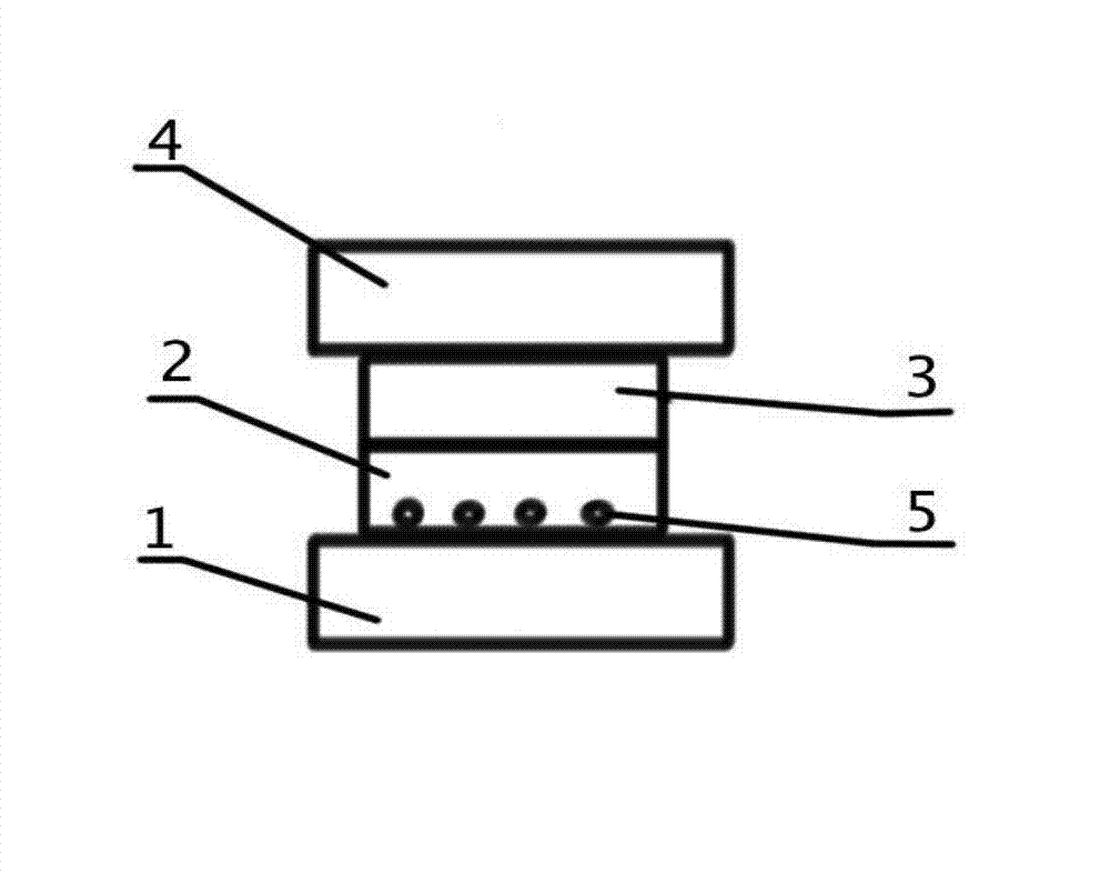
[0021] The resistive variable memory, as shown in the accompanying drawing, includes a lower electrode 1, an induction layer I2, an induction layer II3, an upper electrode 4, and an induction layer I2 in which metal nanocrystalline particles 5 are spontaneously formed; the lower electrode is made of 50nm copper metal, and the induction layer I use 100nm silicon dioxide doped with 3% phosphorus, and the induction layer II uses 100nm silicon dioxide doped with 3% boron; the upper electrode uses 50nm platinum metal.

[0022] The preparation steps of the resistive variable memory are as follows:

[0023] 1) Use PVD (physical vapor deposition) to deposit the lower electrode, which is 50nm thick metal copper;

[0024] 2) Use PVD (physical vapor deposition) to deposit induction layer I with silicon dioxide doped with 3% phosphorus, and its thickness is 100nm;

[0025] 3) Use PVD (physical vapor deposition) to deposit induction layer II silicon dioxide doped with 3% boron, with a thi...

Embodiment 2

[0029] The resistive variable memory, as shown in the accompanying drawing, includes a lower electrode 1, an induction layer I2, an induction layer II3, an upper electrode 4, and an induction layer I2 in which metal nanocrystalline particles 5 are spontaneously formed; the lower electrode is made of 50nm copper metal, and the induction layer 100nm titanium oxide is used for I, 100nm nickel oxide is used for the induction layer II; 50nm platinum metal is used for the upper electrode.

[0030] The preparation steps of the resistive variable memory are as follows:

[0031] 1) Use PVD (physical vapor deposition) to deposit the lower electrode, which is 50nm thick metallic copper;

[0032] 2) The induction layer I titanium oxide is deposited by DC magnetron sputtering method, the process parameters are 100W power, the working pressure is 1Pa, the oxygen partial pressure is 5%, the temperature is 300K, and its thickness is 100nm;

[0033] 3) The induction layer II nickel oxide is d...


PUM

PropertyMeasurementUnit
thicknessaaaaaaaaaa
thicknessaaaaaaaaaa

Abstract

The invention discloses a P/N-type laminated resistive random access memory for growing metal nano crystal particles spontaneously. The P/N-type laminated resistive random access memory for growing metal nano crystal particles spontaneously is composed of a lower electrode, an induction layer I, an induction layer II and an upper electrode which are laminated sequentially. The lower electrode is metal which is easy to be oxidized into a metal ion under the forward electric field effect; the induction layer I is an N-type oxide; the induction layer Ii is a P-type oxide; the upper electrode is a metal or electric conducting compound with stable properties under the electric field effect; the lower electrode grows metal nanocrystalline particles spontaneously in the induction layer I under the forward electric field effect, becomes a lower resistor when a reverse bias voltage is added for the lower electrode, thus the operation of data '1' storage is carried out, and becomes a high resistor when a forward or reverse bias voltage is added for the lower electrode, thus the operation of data '0' storage is carried out. The P/N-type laminated resistive random access memory for growing metal nano crystal particles spontaneously provided by the invention has the advantages that the resistive random access memory acts as an induction factor of an electric conducting channel by utilizing metal nanocrystals; and the number of formed nanocrystals is controlled through the induction layer I, so that the vibration of the voltage and current of a device can be controlled effectively and the controllability of the access memory is improved.

Description

technical field [0001] The invention relates to a preparation process of a non-volatile memory in a microelectronic device, in particular to a P / N type stacked resistance variable memory with spontaneously growing metal nanocrystal particles. Background technique [0002] With the development of technology, information storage devices are becoming more and more important in life. Traditional memories such as SRAM, DRAM, and FLASH are facing the challenge of insurmountable size limits. At the same time, another new storage concept It is gradually considered to be the development direction of future memory devices - RRAM. [0003] RRAM is a new type of storage concept that represents binary by resistance state. It has non-volatility, small device unit, simple structure, low power consumption, fast erasing and writing speed, many repeatable erasing and erasing cycles, and high compatibility with traditional CMOS manufacturing processes. The advantages are currently being exten...

Claims


Application Information

Patent Timeline
Patent Type & Authority Applications(China)
IPC IPC(8): H01L45/00
Inventor 赵金石邵兴隆
Owner TIANJIN UNIVERSITY OF TECHNOLOGY
Why Eureka
Try Eureka