Method for preparing germanium-base MOSFET grate medium

A gate dielectric, germanium-based technology, applied in the field of preparation of germanium-based MOSFET gate dielectric, to achieve the effects of improved electrical characteristics, low interface state density, and high thermal stability

Inactive Publication Date: 2013-02-13
INST OF MICROELECTRONICS CHINESE ACAD OF SCI
View PDF5 Cites 9 Cited by
  • Summary
  • Abstract
  • Description
  • Claims
  • Application Information

AI Technical Summary

Problems solved by technology

However, when the gate length of MOS devices is reduced to 90 nanometers, the thickness of the gate oxide layer is only 1.2 nanometers, and Moore's Law begins to face challenges from both physics and technology.

Method used


Image

  • Method for preparing germanium-base MOSFET grate medium
  • Method for preparing germanium-base MOSFET grate medium
  • Method for preparing germanium-base MOSFET grate medium

Examples


Embodiment Construction

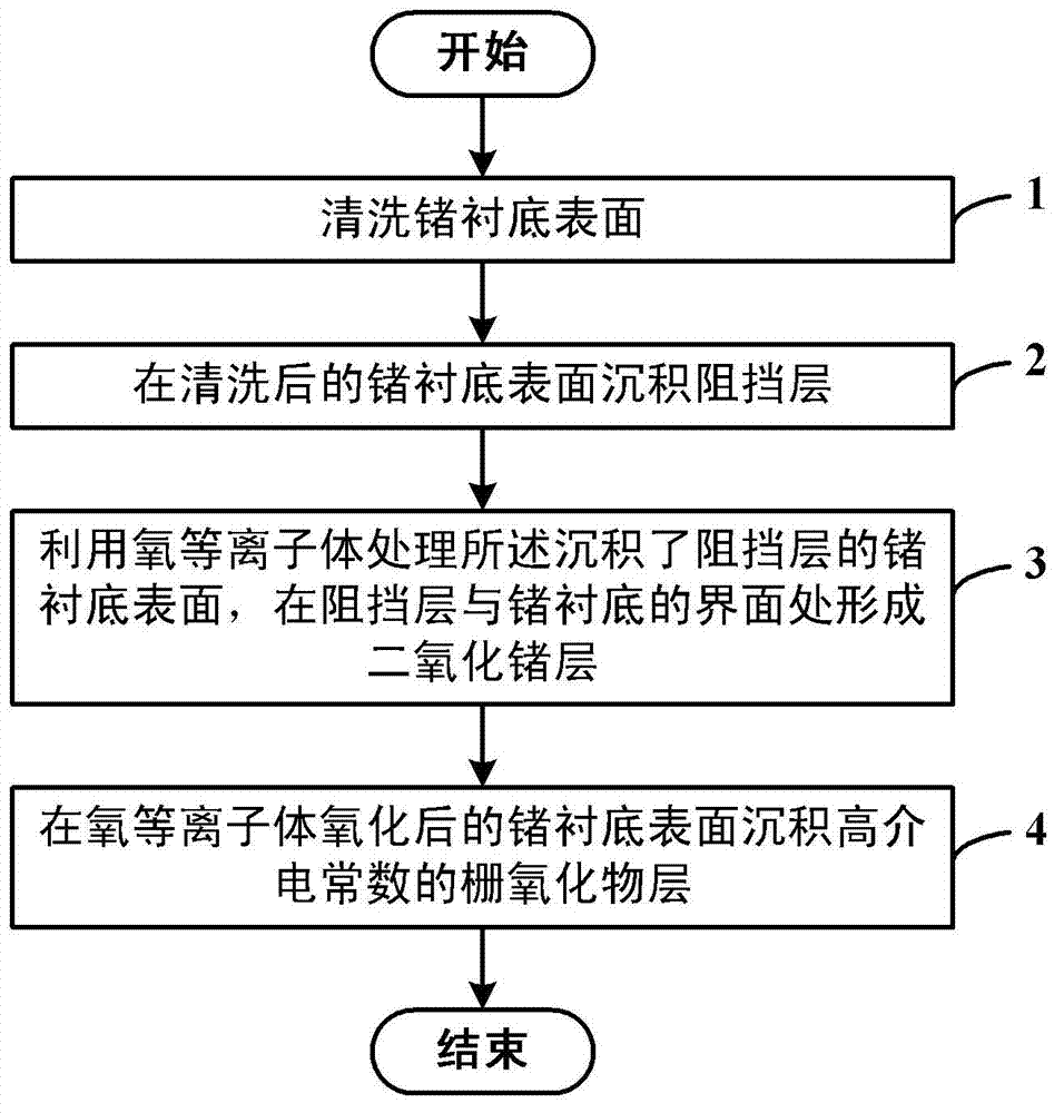
[0017] In order to make the object, technical solution and advantages of the present invention clearer, the present invention will be described in further detail below in conjunction with specific embodiments and with reference to the accompanying drawings.

[0018] The method for preparing a germanium-based MOSFET gate dielectric provided by the present invention adopts lanthanum trioxide with a high dielectric constant as the plasma oxidation protection layer, and uses oxygen plasma to oxidize the surface of germanium to form a thin layer of germanium dioxide, thereby forming a high-quality The oxide-semiconductor interface, and finally depositing a high dielectric constant gate dielectric material on the surface of dilanthanum trioxide to form a composite gate dielectric of germanium dioxide-lanthanum trioxide-high dielectric constant gate dielectric material. The method can reduce the equivalent oxide layer thickness of the germanium-based MOSFET to less than 1 nanometer, t...


PUM


Abstract

The invention discloses a method for preparing a germanium-base MOSFET (Metal-Oxide Semiconductor Field-Effect Transistor) grate medium, which comprises the following steps: Step 1, cleaning the surface of a germanium lining; Step 2, depositing a blocking layer on the cleaned germanium lining; Step 3, utilizing oxygen plasma to process the surface of the germanium lining deposited with the blocking layer, and forming a germanium oxide on the interface of the blocking layer and the germanium lining; and Step 4, depositing a grate oxide layer with high dielectric constant on the surface of the germanium lining oxidized by the oxygen plasma. With the adoption of the method, the equifinal oxide layer thickness of the germanium-base MOSFET can be lowered below 1 nanometer, thereby effectively improving the performance of the germanium-base MOSFET.

Description

technical field [0001] The invention relates to the technical field of semiconductor integration, in particular to a preparation method of a germanium-based MOSFET gate dielectric. Background technique [0002] As the core and foundation of the information industry, semiconductor technology is regarded as an important symbol to measure a country's scientific and technological progress and comprehensive national strength. In the past 40 years, the integrated circuit technology based on silicon-based CMOS technology has followed Moore's law to increase the working speed of the chip, increase the integration level and reduce the cost by reducing the feature size of the device. The feature size of the integrated circuit has evolved from the micron scale. to the nanoscale. However, when the gate length of MOS devices is reduced to 90 nanometers, the thickness of the gate oxide layer is only 1.2 nanometers, and Moore's Law begins to face challenges from both physics and technolog...

Claims


Application Information

Patent Timeline
Patent Type & Authority Applications(China)
IPC IPC(8): H01L21/28
Inventor 孙兵刘洪刚王盛凯赵威
Owner INST OF MICROELECTRONICS CHINESE ACAD OF SCI
Why Eureka
Try Eureka