Structure of perpendicular asymmetric ring gating metal oxide semiconductor field effect transistor (MOSFET) device and manufacturing method thereof

An asymmetric and device technology, applied in the formation of semiconductor devices, the structure and manufacture of vertical asymmetric gate-around MOSFET devices, can solve large junction leakage current, reduce channel carrier mobility, and insufficient gate control capability and other issues, to achieve the effect of enhancing gate control capability and superior device performance

Inactive Publication Date: 2013-02-13
三亚哈尔滨工程大学南海创新发展基地
View PDF6 Cites 1 Cited by
  • Summary
  • Abstract
  • Description
  • Claims
  • Application Information

AI Technical Summary

Problems solved by technology

[0004] However, when the channel length is reduced to less than 50 nanometers, vertical structure MOSFET devices will face a serious problem: in order to suppress the short channel effect, the channel doping concentration must be very high (up to 7.0×10 18 cm -3 ), which will lead to a large junction leakage current and reduce the channel carrier mobility
Compared with the device structure proposed by the present invention, the above two devices have the disadvantages of insufficient gate control capability and excessive leakage current

Method used


Image

  • Structure of perpendicular asymmetric ring gating metal oxide semiconductor field effect transistor (MOSFET) device and manufacturing method thereof
  • Structure of perpendicular asymmetric ring gating metal oxide semiconductor field effect transistor (MOSFET) device and manufacturing method thereof
  • Structure of perpendicular asymmetric ring gating metal oxide semiconductor field effect transistor (MOSFET) device and manufacturing method thereof

Examples


specific Embodiment 1

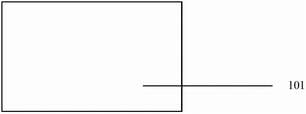
[0033] combine figure 2 . As shown, an n-type silicon wafer substrate 101 with crystal orientation is prepared with a thickness of 100 nm.

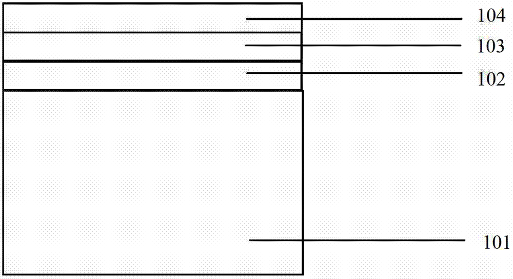
[0034] combine image 3 . On the n-type silicon wafer 101, SiO is sequentially deposited 2 layer 102, SiGe layer 103 and SiO 2 Layer 104. Of which SiO 2 layer 102, SiGe layer 103 and SiO 2 The thickness of the layer 104 is 20-50 nm.

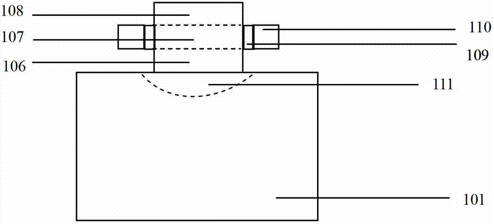
[0035] combine Figure 4 . right image 3 The structure is photolithographically made so that the middle part of the SiO 2 layer 102, SiGe layer 103 and SiO 2 Layer 104 is etched away in its entirety, forming a window. Then, the photoresist is used as a doping mask layer to perform n-type doping implantation on the silicon material, and rapid thermal annealing (RTA) activates the impurities to form the drain region 111 .

[0036] combine Figure 5 . The epitaxial silicon layer 105 is epitaxial on the silicon material, and the thickness of the epitaxial silicon layer 105 is 200-300nm. At the...

Embodiment 1

[0041] The advantages of Embodiment 1 are: 1) the gate-around structure is adopted, and the effective number of gates is the largest, so the gate has the strongest electrical control over the channel, and the short channel effect can be minimized; 2) the vertical channel is adopted Structure, no need to use complex lithography means to define the channel length, not limited by lithography accuracy, and the working principle and characteristics are almost the same as planar devices; 3) Using asymmetric LDD structure, compared with symmetric LDD structure, it can It has the advantages of reducing the cut-off leakage current, reducing the electric field near the drain junction, suppressing the short channel effect and reducing the series resistance of the source terminal. The manufacturing process is compatible with the planar CMOS process and is easy to implement; 4) Using the gate-last process, first perform self-aligned doping to form the source region, channel region and drain...

specific Embodiment 2

[0042] Other described steps are the same as the specific embodiment one.

[0043] combine Figure 7 . SiO 2 Layer 104 is a masking layer. Firstly, low-energy ion implantation is performed, the implantation energy is 20keV, and the dose is 5×10 13 cm -2 boron ions to form a graded channel; then perform high-energy ion implantation with an implantation energy of 20keV and a dose of 2×10 15 cm -2 of arsenic ions to form the source region. Rapid thermal annealing is then performed to activate the impurities. The doping concentration of the gradient channel region 107 gradually decreases from the source end to the drain end, which is 2×10 18 ~8×10 17 cm -3 .


PUM


Abstract

The invention provides a structure of a perpendicular asymmetric ring gating metal oxide semiconductor field effect transistor (MOSFET) device and a manufacturing method thereof. The structure of the device comprises a bottom-layer n-type silicon wafer substrate 101, wherein a drain region 111 is positioned at the bottommost end of the device; a drain expansion region 106, a channel region 107 and a source region grow on the substrate 101 in an epitaxial manner; a grating oxidization layer 109 encircles the whole channel region 107; and polycrystalline silicon gratings 110 are deposited on the grating oxidization layer 109. The invention provides the structure of the perpendicular asymmetric ring gating MOSFET with a function of effectively suppressing a short channel effect and a manufacturing method of the perpendicular asymmetric ring gating MOSFET; and by the manufacturing method, the technical process can be simplified and the length of the grating and the thickness of a silicon body region can be flexibly controlled.

Description

technical field [0001] The invention relates to a semiconductor device, and the invention also relates to a method for forming the semiconductor device. Specifically, it is a structure and a manufacturing method of a vertical asymmetric ring gate MOSFET device. Background technique [0002] In recent years, with the rapid development of the semiconductor industry, integrated circuits have developed into very large scale integrated circuits (ULSI) stage. The size of the device is also reduced to the nanometer level, which poses a great challenge for the development of new device structures and fabrication processes. Over the past few decades, the size of MOSFET devices has been continuously reduced, and today the effective channel length of MOSFET devices is less than 10 nanometers. In order to continuously improve the current driving ability and better suppress the short channel effect, MOSFET devices have developed from traditional single-gate planar devices to multi-gate...

Claims


Application Information

Patent Timeline
Patent Type & Authority Applications(China)
IPC IPC(8): H01L29/78H01L29/423H01L21/336
CPCH01L29/66666H01L29/7827
Inventor 王颖单婵曹菲邵雷
Owner 三亚哈尔滨工程大学南海创新发展基地
Why Eureka
Try Eureka