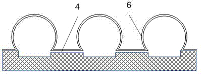
Manufacturing method for size-controllable wafer level glass micro-cavity
A wafer-level, glass micro-technology, applied in micro-structure technology, micro-structure devices, manufacturing micro-structure devices, etc., can solve the problems of ultra-clean room pollution, affecting the reliability of micro-electronic devices, and difficult to accurately quantify weighing
- Summary
- Abstract
- Description
- Claims
- Application Information
AI Technical Summary
Problems solved by technology
Method used
Image
Examples
Embodiment 1
[0028] A method for preparing a wafer-level glass microcavity with a controllable size, comprising the following steps:
[0029] In the first step, an array of micro silicon grooves is etched on a silicon wafer (for example, a 4-inch silicon wafer), and the micro silicon grooves are connected by microchannels. The silicon wafers used may be standard thickness silicon wafers, eg, 500 micrometer thick silicon wafers. The depth of the micro silicon groove is 10-300 microns, such as 15 microns, 30 microns, 60 microns, 100 microns, 150 microns, 180 microns, 200 microns, 300 microns, and the aspect ratio is usually less than 2, for example, it can be selected as 1.5 , 1, 0.8, 0.5, 0.2, 0.1, 0.05, 0.01, the microfabrication process of the pattern structure on the silicon wafer is wet etching process, dry inductively coupled plasma (ICP) etching process or reactive ion etching process One of them, preferably a wet etching process, such as etching with TMAH solution, the pattern can b...
Embodiment 2
[0036] A method for preparing a wafer-level glass microcavity with a controllable size, comprising the following steps:
[0037] The first step is to etch micro silicon grooves on a 4-inch silicon wafer. The micro silicon grooves are connected through microchannels. The silicon wafer used is a standard thickness silicon wafer with a thickness of 500 microns. The depth of the micro silicon groove is 150 micron, micro silicon grooves are square grooves with a diameter of 2 mm. The micromachining process of the pattern structure on the silicon wafer is a wet etching process, and the etching solution used is a 25% TMAH solution, and the temperature is 90°C;
[0038] In the second step, a certain amount of sodium carbonate solution and calcium chloride solution (at room temperature of 25 degrees Celsius) are quantitatively injected into the micro silicon groove by dispensing technology successively, and after evaporation, calcium carbonate crystals are finally obtained. . Then ad...
PUM
| Property | Measurement | Unit |
|---|---|---|
| depth | aaaaa | aaaaa |
| thickness | aaaaa | aaaaa |
| depth | aaaaa | aaaaa |
Abstract
Description
Claims
Application Information


