OLED (Organic Light Emitting Diode) device working under low voltage
A low-voltage, device technology, applied in the field of OLED devices, can solve the problems of device driving voltage increase, restricted mobility, etc.
- Summary
- Abstract
- Description
- Claims
- Application Information
AI Technical Summary
Problems solved by technology
Method used
Image
Examples
Embodiment 1
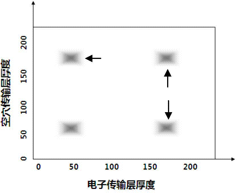
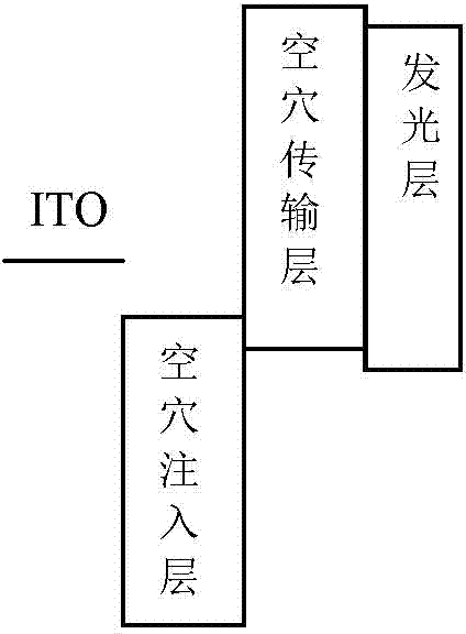
[0070] see image 3 The partial structural diagram of the inverted OLED device of the shown embodiment 1, embodiment 1 is a kind of green light-emitting device, adopts ITO as cathode, Alq 3 Doped cesium carbonate (cesium obtained by thermal decomposition) as electron injection layer, Alq 3 As the electron transport layer, AND doped C545T as the green light-emitting layer; NPB as the hole transport layer; HAT-cn as the hole injection layer. Alq 3 As an electron transport layer; LiF as an electron injection layer; Al as a metal anode layer. The device structure of this embodiment is as follows:
[0071] ITO / Alq 3 :10%Cs 2 CO 3 (20nm) / Alq 3 (5nm) / ADN: 2%C545T(30nm) / NPB(10nm) / HAT-cn(20nm) / Al(150nm) (1).
[0072] The specific preparation method for preparing the organic electroluminescent device with the above structural formula (1) is as follows:
[0073] The glass substrate was cleaned by detergent ultrasonic and deionized water ultrasonic, and dried under an infrared la...
Embodiment 2
[0090] Example 2 (see Figure 7 ):
[0091] Embodiment 2 is a blue light-emitting device of the present invention, using ITO as the cathode, Alq 3 Doped cesium carbonate (cesium obtained by thermal decomposition) as electron injection layer, Alq 3 As the electron transport layer, AND doped TBPe as the blue light-emitting layer; NPB as the hole transport layer; HAT-cn as the hole injection layer. Alq 3As an electron transport layer; LiF as an electron injection layer; Al as a metal anode layer. The device structure of this embodiment is as follows:
[0092] ITO / Alq 3 :10%Cs 2 CO 3 (20nm) / Alq 3 (5nm) / ADN:3%TBPe(30nm) / NPB(10nm) / HAT-cn(20nm) / Al(150nm) (2)
[0093] The preparation process of Example 2 is: using dual-source evaporation to prepare an AND and TBPe doped layer with a thickness of 30 nm and a TBPe doping ratio of 3%.
[0094] Evaporate 10nm thick NPB as a hole injection layer, and cover 20nm HAT-cn as a hole injection layer. Finally, 150 nm of Al was vapor-de...
Embodiment 3
[0104] Embodiment 3 (see Figure 11 ):
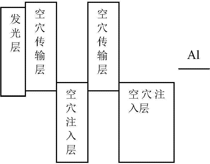
[0105] Embodiment 3 is a blue light-emitting device of the present invention, using ITO as the cathode, Alq 3 Doped cesium carbonate (cesium obtained by thermal decomposition) as electron injection layer, Alq 3 As the electron transport layer, AND doped TBPe as the blue light-emitting layer; NPB as the hole transport layer; HAT-cn as the hole injection layer. Alq 3 As an electron transport layer; LiF as an electron injection layer; Al as a metal anode layer. The device structure of this embodiment is as follows:
[0106] ITO / Alq 3 :10%Cs 2 CO 3 (20nm) / Alq 3 (5nm) / ADN: 3%TBPe(30nm) / NPB(20nm) / HAT-cn(20nm) / NPB(20nm) / HAT-cn(70nm) / Al(150n) (3).
[0107] The preparation process of Example 3 is: using dual-source evaporation to prepare an AND and TBPe doped layer with a thickness of 30 nm and a TBPe doping ratio of 3%.
[0108] Evaporate 20nm thick NPB as the hole injection layer, and at the same time cover 20nm HAT-cn as the hole in...
PUM
 Abstract
Description
Claims
Application Information


