Method of producing formed circuit component

A manufacturing method and a technology for forming circuits, which are applied in the fields of printed circuit manufacturing, printed circuit parts, printed circuits, etc., can solve problems such as roughening, laboriousness, and reduced insulation, and achieve enhanced adhesion, improved durability or durability. Thermal properties, the effect of improving the anchoring effect

Inactive Publication Date: 2013-04-17
SANKYO KASEI CO LTD
View PDF8 Cites 38 Cited by
  • Summary
  • Abstract
  • Description
  • Claims
  • Application Information

AI Technical Summary

Problems solved by technology

Further, in order to selectively roughen the surface of the substrate by chemical etching, it is necessary to cover the surface that is not to be roughened with a mask, which is a laborious work.
In addition, when roughening the entire surface of the substrate by chemical etching, in order to apply catalyst and electroless plating only to t

Method used


Image

  • Method of producing formed circuit component
  • Method of producing formed circuit component

Examples


Embodiment 1

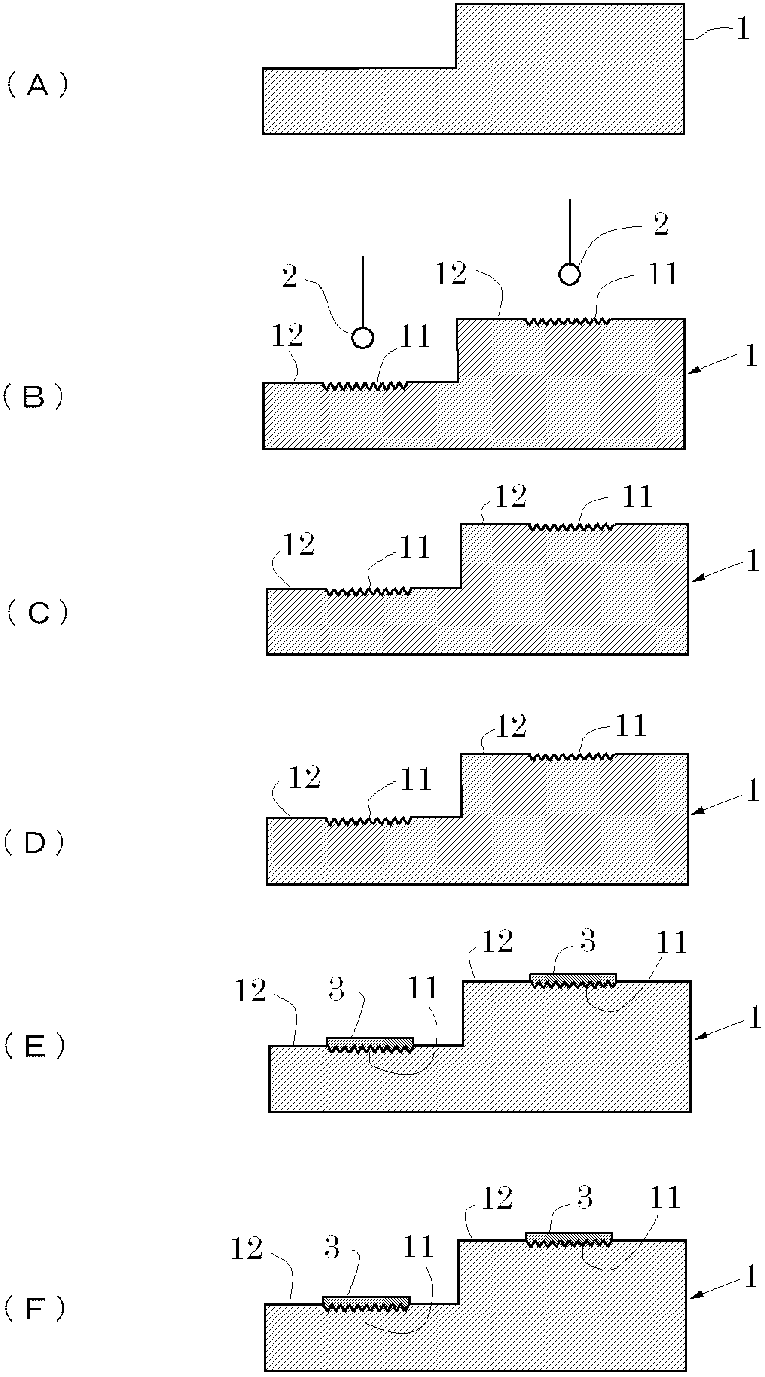
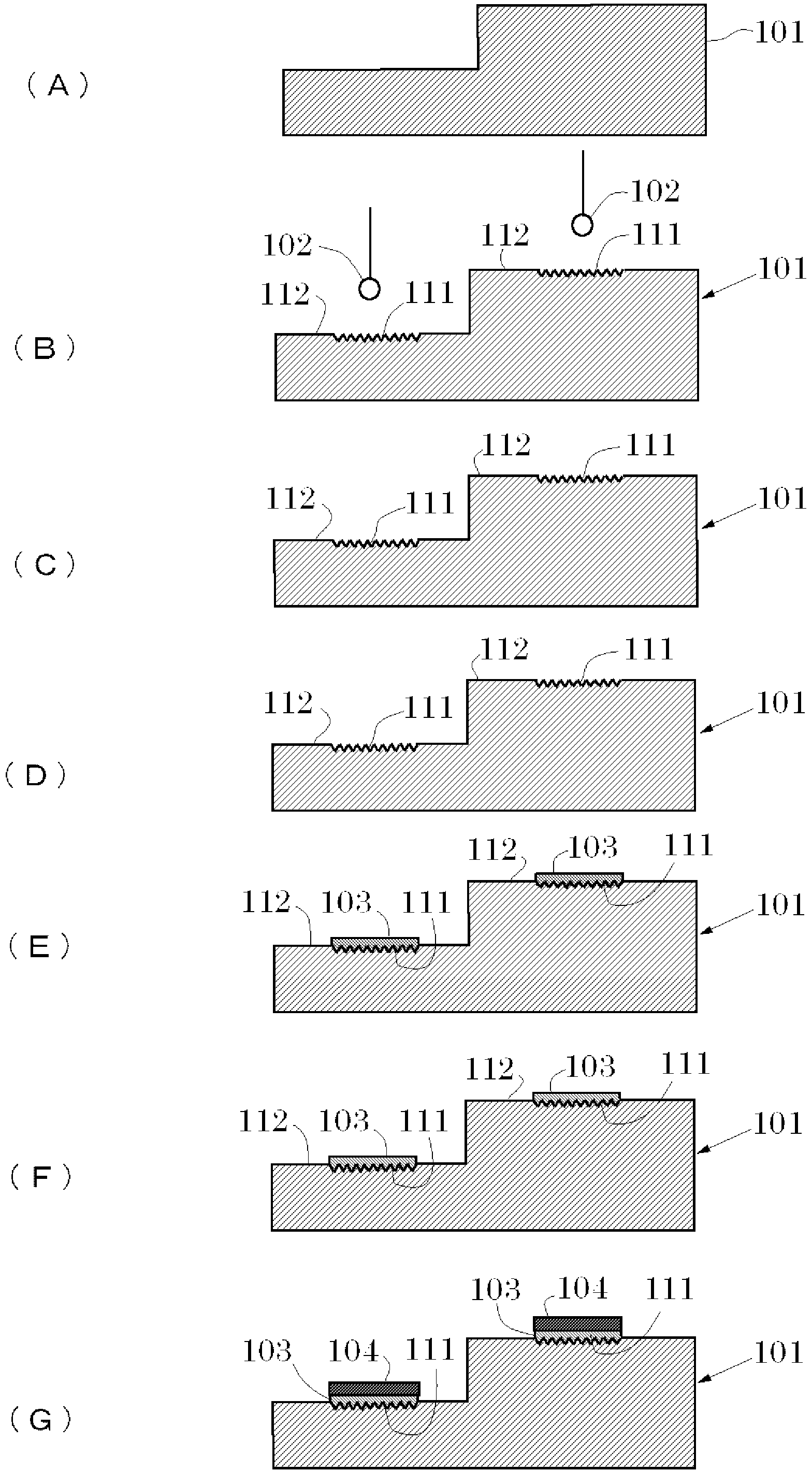
[0057]An aromatic polyamide (6T nylon) (manufactured by Otsuka Chemical Co., Ltd. "#NM114HW") mixed with titanium oxide and calcium titanate whiskers as a filler was injection-molded to form a bulk-shaped base 1 . Next, the laser beam 2 is selectively irradiated to the circuit portion 11 of the substrate 1 to modify and roughen the surface. The laser beam 2 uses the second harmonic wave with a wavelength of 532nm, and the output is 95% of 6W. According to the scanning speed of the galvanometer mirror, the scanning speed is 500mm / s, and the pulse frequency is set at 40KHz, and only one scanning is performed. It was confirmed that the 10-point average of the roughness of the surface that can be roughened by this was about 84 μm.

[0058] Then the substrate 1 is subjected to alkali washing, and then the surface is activated. Here, the alkali cleaning is performed, for example, by immersing the substrate 1 in an aqueous sodium hydroxide solution having a temperature of 50° C. and...

Embodiment 2

[0063] An aromatic liquid crystal polymer ("Bectra #C820" manufactured by Polyplastics Co., Ltd.) mixed with 50% by weight of calcium pyrophosphate as a filler was injection-molded to form a bulk-shaped substrate 1 . Next, the laser beam 2 is selectively irradiated to the circuit portion 11 of the substrate 1 to modify and roughen the surface. The laser beam 2 uses the second harmonic wave with a wavelength of 532nm, and the output is 95% of 6W. The scanning speed of the galvanometer mirror is 100mm / sec, and the pulse frequency is set at 40KHz, and only one scan is performed. It was confirmed that the 10-point average of the roughness of the surface that can be roughened by this was about 115 μm.

[0064] Next, the substrate 1 was subjected to alkali washing in the same manner as in Example 1 to activate the surface, and after the palladium ion catalyst was adsorbed, it was reduced to palladium metal. At this time, it was confirmed that palladium metal was not fixed to the po...

Embodiment 3

[0067] An aromatic liquid crystal polymer (manufactured by Sumitomo Osaka Sement Co., Ltd., "Jima Inas #3Wriflor") to which alumina was added as a filler was injection-molded to form a bulk-shaped substrate 1 . Next, the same laser beam 2 as in Example 2 was selectively irradiated to the portion 11 of the substrate 1 to be a circuit to modify and roughen the surface. It was confirmed that the 10-point average of the roughness of the surface that can be roughened by this was about 306 μm.

[0068] Next, the substrate 1 was subjected to alkali washing in the same manner as in Example 1 to activate the surface, and after the palladium ion catalyst was adsorbed, it was reduced to palladium metal. At this time, it was confirmed that palladium metal was not fixed to the portion 12 not to be a circuit that had not been roughened by the laser beam. It should be noted that the substrate 1 on which palladium metal was adsorbed was activated using the same surfactant as in Example 1. N...


PUM

PropertyMeasurementUnit
Adhesive strengthaaaaaaaaaa

Abstract

An electroless plating layer with strong adhesion is optionally formed only on a portion to be a circuit, and other non-circuit portions are not roughened. A laser beam (2) with a wavelength of 405-1064nm is optionally irradiated onto the portion to be a circuit (11) of a synthetic resin substrate (1), and an ionic catalyst of palladium is caused to be adsorbed and then reduced to metallic palladium by a reducing agent. Subsequently, an electroless plating layer (3) is formed on the portion to be a circuit (11). Since the portion to be a circuit (11) is surface modified and roughened, the ionic catalyst firmly attaches, and the electroless plating layer (3) strongly adheres. The ionic catalyst does not adsorb onto the non-circuit portions (12) not irradiated by the laser beam (2), and thus the electroless plating layer (3) is not formed thereon.

Description

technical field [0001] The present invention relates to a manufacturing method of a shaped circuit part, which selectively forms an electroless plating layer on a roughened synthetic resin surface by irradiation of a laser beam. Background technique [0002] When electroless plating is selectively applied to the surface of a base made of synthetic resin to form a conductive circuit, it is necessary to roughen the surface of the base in advance in order to improve the adhesion with the electroless plating. As this surface roughening method, there is chemical etching using hexavalent chromium sulfate (for example, refer to Patent Document 1). [0003] However, since hexavalent chromium is toxic, the work environment is poor. In addition, in order to safely dispose of the drain of the used etching solution, it is necessary to neutralize and precipitate the hexavalent chromium after reducing it to trivalent chromium, which requires very complicated treatment. Therefore, hexava...

Claims


Application Information

Patent Timeline
IPC IPC(8): H05K3/18C23C18/06C23C18/16C23C18/38H05K1/03H05K3/38
CPCC23C18/1608C23C18/1612C23C18/1635C23C18/1641C23C18/1651C23C18/1653C23C18/1692C23C18/204C23C18/2086C23C18/30C23C18/38C25D3/38H05K1/0284H05K3/0032H05K3/182H05K3/381H05K2201/09118H05K2203/0709
Inventor 汤本哲男渡边充广斋藤裕一
Owner SANKYO KASEI CO LTD
Why Eureka
Try Eureka