Micro/nanometer secondary surface array and preparation method and application thereof

A micro-nano and array technology, applied in the field of micro/nano secondary arrays and its preparation, can solve the problems of difficult control of material microstructure, difficult large-scale production and preparation, light absorption performance attenuation, etc., to reduce the recombination of holes and electrons Chance, low cost, reduce the effect of reflection

Inactive Publication Date: 2013-06-12
SUN YAT SEN UNIV
View PDF3 Cites 6 Cited by
  • Summary
  • Abstract
  • Description
  • Claims
  • Application Information

AI Technical Summary

Problems solved by technology

However, the one-dimensional semiconductor nanoarrays prepared by these methods are regularly arranged, and the light absorption of the vertically incident light is more than that of the thin film, but when the incident angle of the light changes, its light absorption performance will be significantly reduced. At the same time, these preparation methods are relatively complicated, and the main common problems are that it is difficult to realize large-scale production and preparation, the preparation cost is high, and the microstructure of the material is difficult to control.
[0004] According to the existing literature, although the prepared one-dimensional semiconductor nanoarray can improve the light absorption performance, the light absorption performance will rapidly decay with the change of the incident light angle.
At present, there is no method for the preparation of semiconductor nanoarrays with simple process, low production cost, large area, insensitive to light incident angle, and large specific surface area.

Method used


Image

  • Micro/nanometer secondary surface array and preparation method and application thereof
  • Micro/nanometer secondary surface array and preparation method and application thereof
  • Micro/nanometer secondary surface array and preparation method and application thereof

Examples


Embodiment 1

[0032] a Cu 2 S "cactus" micro-nano secondary array is prepared by the following steps:

[0033] (1) Grind the copper sheet with No. 0-6 sandpaper, and then ultrasonically clean it with alcohol, acetone, and deionized water for 5 minutes; then use a potential of -0.35V relative to the saturated calomel electrode on the copper sheet, and deposit at a constant voltage for 2400s A copper film with a spherical crown periodic undulating structure is deposited on the copper sheet;

[0034] (2) Mix the product of step (1) with oxygen / hydrogen sulfide mixed gas (the volume ratio of the two is 1:2), heat at 20°C for 16h, and generate Cu 2 S "cactus" micro-nano secondary array;

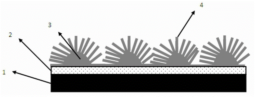
[0035] Cu produced 2 S "cactus" micro-nano secondary array, its structure is as follows figure 1 Shown: On the substrate 1 is a conductive film 2, and above the conductive film 2 are periodically distributed micron-sized Cu 2 S spherical crown 3, Cu 2 The surface of the S spherical cap 3 is nano-sized Cu ...

Embodiment 2

[0038] a Cu 2 S "cactus" micro-nano secondary array is prepared by the following steps:

[0039] (1) The glass sheet is ultrasonically cleaned with 1mol / L NaOH, 1mol / L HCl solution, absolute ethanol, and deionized water in sequence, and then a layer of ITO is magnetron sputtered on the glass sheet with a thickness of 200nm. Deposit a layer of copper film with a spherical crown periodic undulation structure by constant pressure method, and the thickness of the copper film is 500nm;

[0040] (2) Mix the product of step (1) with oxygen / hydrogen sulfide mixed gas (the volume ratio of the two is 1:2), heat at 10°C for 18h, and generate Cu 2 S "cactus" micro-nano secondary array;

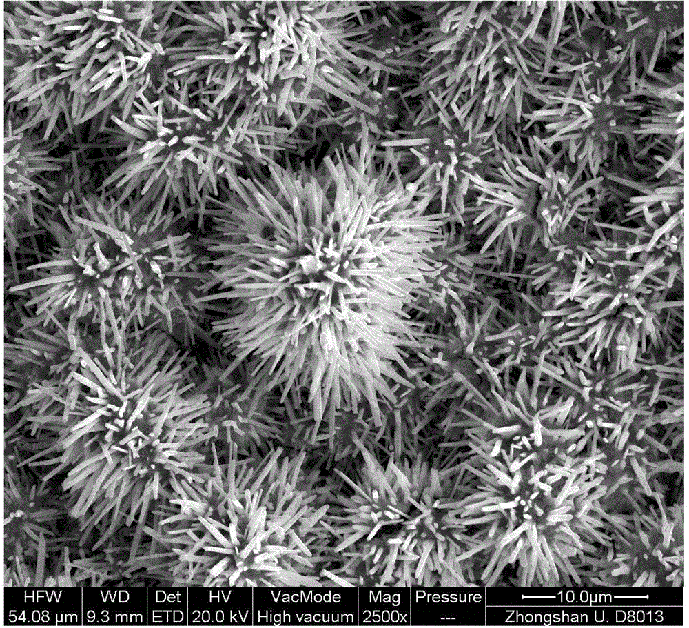
[0041] Cu produced 2 S "cactus" micro-nano secondary, its structure is as follows figure 1 shown. The diameter of the nanowire is 40nm, the length is 5um, Cu 2 The diameter of the S spherical cap is 5μm, and the interval between the spherical caps is 2um. The prepared Cu 2 The scanning electron mic...

Embodiment 3

[0044] a Cu 2 S "cactus" micro-nano secondary array is prepared by the following steps:

[0045] (1) Clean the silicon wafer sequentially with 1mol / L NaOH, 1mol / L HCl solution, absolute ethanol, and deionized water; then thermally evaporate a layer of Au film on the silicon wafer with a thickness of 200nm, and then Deposit a layer of copper film with spherical crown periodic undulation structure by pulse electrochemical deposition method, the thickness of copper film is 800nm;

[0046] (2) Mix the product of step (2) with oxygen / hydrogen sulfide mixed gas (the volume ratio of the two is 1:2), heat at 18°C ​​for 12h, and generate Cu 2 S "cactus" micro-nano secondary array;

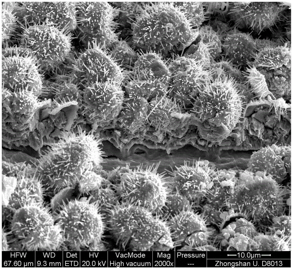
[0047] Cu produced 2 S "cactus" micro-nano secondary array, its structure is as follows figure 1 shown. The diameter of the nanowire is 100nm, the length is 12um, Cu 2 The diameter of the S spherical cap is 8μm, and the interval between the spherical caps is 5um. The prepared Cu 2 The scanning electr...


PUM

PropertyMeasurementUnit
diameteraaaaaaaaaa
lengthaaaaaaaaaa
lengthaaaaaaaaaa

Abstract

The invention discloses a 'cactus' micro / nanometer secondary surface array structure, a preparation method and application of the 'cactus' micro / nanometer secondary surface array structure. The micro / nanometer secondary surface array is formed in the manner that nanoscale copper 2 sulphur (Cu2S) nanometer lines grow on the surface of micron scale Cu2S spherical crowns, and the Cu2S spherical crowns are periodically distributed on the surface of a substrate. Compared with a common plane nanometer line array, the Cu2S'cactus' micro / nanometer secondary surface array further increases specific surface area, and increases probability of generation of charge carriers. Meanwhile, when the angle of incident light changes, change of relative position between the nanometer lines and light rays is small, and change of light absorption is small, so the light absorption can maintain good performance within the wide light incident angle. When the Cu2S'cactus' micro / nanometer secondary surface array is applied to the field of solar energy, the Cu2S'cactus' micro / nanometer secondary surface array can overcome the defects of degrading the performance along with the position of the sun, or changing angles of devices continuously along with the change of illumination angles to cause complexity of structure of the devices and increase of cost.

Description

technical field [0001] The invention belongs to the application field of material surface light absorption, in particular to a Cu 2 Micro / nano secondary array formed by S "cactus" and its preparation method and application. Compared with the planar nanowire array, the "cactus" micro-nano secondary array has a larger specific surface area. This structure still maintains good surface light absorption performance when the incident angle of light changes, and can be widely used in the fields of photovoltaic and photothermal energy conversion. At the same time, the preparation method has the advantages of low cost, simple method, suitable for large area growth and preparation, and the like. Background technique [0002] The special properties of nanomaterials are often related to their shape and size. Among them, one-dimensional nanomaterials, especially one-dimensional semiconductor nanoarrays, have attracted more attention in photoelectric conversion applications due to their ...

Claims


Application Information

Patent Timeline
Patent Type & Authority Applications(China)
IPC IPC(8): H01L31/0352H01L31/18F24J2/48
CPCY02E10/40Y02P70/50
Inventor 任山李立强李明刘珠凤洪澜
Owner SUN YAT SEN UNIV
Why Eureka
Try Eureka