Semiconductor porous bismuth oxide nanosphere and preparation method and application thereof

A semiconductor and nanosphere technology, applied in the field of nanomaterials and photocatalysis, can solve the problems of nanomaterial morphology, less size synthesis route, no spherical nanostructure, and difficulty in liquid phase synthesis, etc., which is conducive to market promotion, excellent The effect of degradation performance and good cycle stability

Inactive Publication Date: 2013-08-21
WUHAN UNIV OF TECH
View PDF5 Cites 9 Cited by
  • Summary
  • Abstract
  • Description
  • Claims
  • Application Information

AI Technical Summary

Problems solved by technology

However, due to the low melting point of bismuth, it is not easy to synthesize by gas phase method, and there are relatively few sources of bismuth, generally only Bi(NO 3 ) 3 ·5H 2 O and BiCl 3 And it is easy to hydrolyze, difficult to dissolve in aqueous solution, and difficult to synthesize by liquid phase method, so it is difficult to efficiently prepare Bi by traditional gas-solid-liquid method. 2 o 3 , so that Bi 2 o 3 There are relatively few synthetic routes with controllable morphology, size and crystal form of nanomaterials
And Bi 2 o 3 More inclined to self-nucleation, easy to generate sheet-like structure
Currently, there is no Bi 2 o 3 Reports on Spherical Nanostructures

Method used


Image

  • Semiconductor porous bismuth oxide nanosphere and preparation method and application thereof
  • Semiconductor porous bismuth oxide nanosphere and preparation method and application thereof
  • Semiconductor porous bismuth oxide nanosphere and preparation method and application thereof

Examples


Embodiment 1

[0033] The preparation of porous bismuth oxide nanospheres of semiconductor photocatalytic materials by soft film plate method comprises the following steps:

[0034] 1) Add 0.076g (1.567*10 -4 mol) bismuth nitrate pentahydrate and 25ml deionized water to make a solution, and 0.21g (4.88*10 -4 mol) sodium cholate and 10ml deionized water to make a solution, mix and stir the two solutions evenly to obtain a 35ml solution;

[0035] 2) Add 1ml of hydrogen peroxide to the above mixed solution, transfer the obtained mixed solution into a reaction kettle, and react at 200°C for 8 hours to obtain a khaki precursor solution;

[0036] 3) Cool the obtained precursor solution naturally, wash it, and place it in an oven at 60°C until it is completely dried;

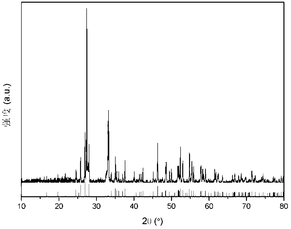
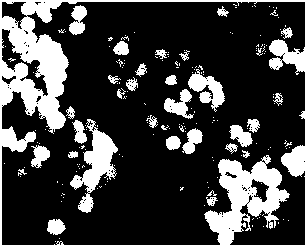
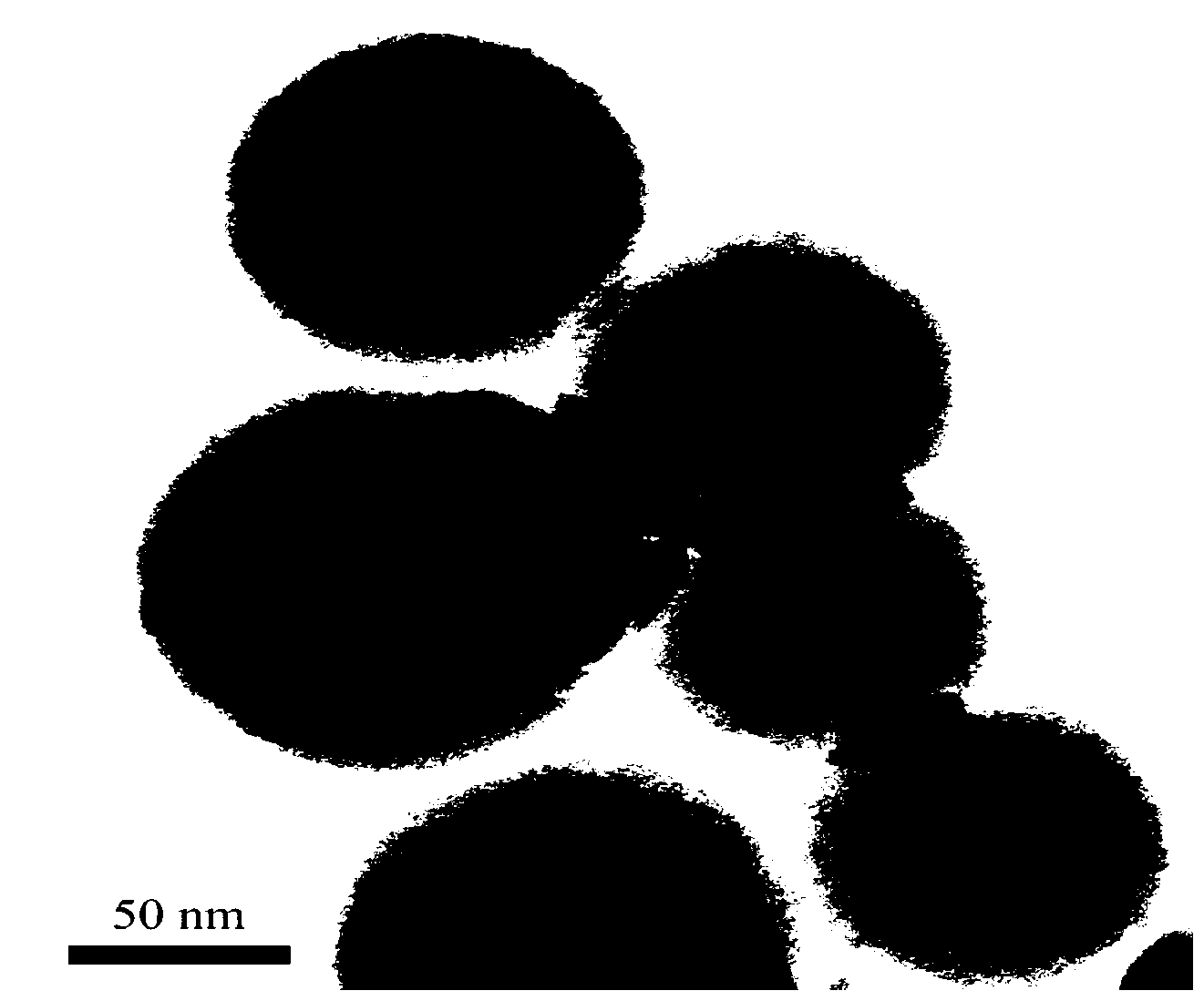
[0037] 4) Grind the precursor obtained after drying evenly, put it into a tube furnace, and calcinate it at 500°C for 2 hours in an air atmosphere to obtain a yellow powder that is bismuth oxide nanospheres.

[0038] Taking bismut...

Embodiment 2

[0044] The preparation of porous bismuth oxide nanospheres of semiconductor photocatalytic materials by soft film plate method comprises the following steps:

[0045] 1) Make a solution of 0.06g of bismuth nitrate pentahydrate and 15ml of deionized water, and make a solution of 0.21g of sodium cholate and 10ml of deionized water, mix and stir the two solutions to obtain a 25ml solution;

[0046] 2) Add 0.5ml hydrogen peroxide to the above mixed solution, transfer the obtained mixed solution into a reaction kettle, and react at 200°C for 8 hours to obtain a khaki precursor solution;

[0047]3) Cool the obtained precursor solution naturally, wash it, and place it in an oven at 60°C until it is completely dried;

[0048] 4) Grind the precursor obtained after drying evenly, put it into a tube furnace, and calcinate it at 500°C for 2 hours in an air atmosphere to obtain a yellow powder that is bismuth oxide nanospheres.

[0049] The bismuth oxide nanosphere material prepared by th...

Embodiment 3

[0051] The preparation of porous bismuth oxide nanospheres of semiconductor photocatalytic materials by soft film plate method comprises the following steps:

[0052] 1) Make a solution of 0.076g of bismuth nitrate pentahydrate and 25ml of deionized water, and make a solution of 0.202g of sodium cholate and 5ml of deionized water, mix and stir the two solutions to obtain a 30ml solution;

[0053] 2) Add 1.5ml of hydrogen peroxide to the above mixed solution, transfer the obtained mixed solution into a reaction kettle, and react at 200°C for 9 hours to obtain a khaki precursor solution;

[0054] 3) Cool the obtained precursor solution naturally, wash it, and place it in an oven at 60°C until it is completely dried;

[0055] 4) Grind the precursor obtained after drying evenly, put it into a tube furnace, and calcinate it at 500°C for 2 hours in an air atmosphere to obtain a yellow powder that is bismuth oxide nanospheres.

[0056] The bismuth oxide nanosphere material prepared ...


PUM

PropertyMeasurementUnit
diameteraaaaaaaaaa

Abstract

The invention relates to a preparation method for a visible-light-responsive photocatalytic semiconductor material. The semiconductor material is a nanosphere with a uniform porous structure, a uniform size, good dispersibility and a diameter of 60 to 120 nm. A preparation method for the semiconductor material comprises the following steps: 1) preparing a solution from a bismuth source and deionized water and adding a surfactant into the solution; 2) adding hydrogen peroxide into a mixed solution obtained in step 1), transferring an obtained solution into a reaction vessel and carrying out a reaction so as to obtain an earthy yellow precursor solution; 3) subjecting the obtained precursor solution to natural cooling at first and then to washing and carrying out drying with a baking oven; and 4) uniformly grinding a precursor obtained after drying and calcining the ground precursor in a tubular furnace. The invention has the following beneficial effects: as a material for degradation of pollutants, the semiconductor material shows excellent degradation performance, a narrow energy band gap and good cycling stability. The preparation method is simple, accords with requirements for green chemistry and is beneficial for market popularization.

Description

technical field [0001] The invention belongs to the field of nanometer materials and photocatalysis, and in particular relates to a preparation method of a visible light responsive nanometer photocatalytic semiconductor material. The photocatalytic material can be used to degrade pollutants under visible light. Background technique [0002] With the progress of society and the rapid development of economy, the pollution of the environment is becoming more and more serious. Semiconductor photocatalytic materials have attracted much attention because of their potential applications in converting sunlight energy and degrading pollutants. Since Fujishima and Honda reported on Nature in 1972 that TiO 2 Since single crystals can be used as electrodes to photodecompose water to produce hydrogen at room temperature, semiconductor photocatalytic materials have attracted the attention of researchers. At present, research on the more mature semiconductor materials, TiO 2 、 Ta 2 o 5...

Claims


Application Information

Patent Timeline
Patent Type & Authority Applications(China)
IPC IPC(8): C01G29/00B01J23/18B01J35/10B01J13/02B82Y40/00B82Y30/00
Inventor 施伟东官建国孙晓莉
Owner WUHAN UNIV OF TECH
Why Eureka
Try Eureka