Photonic crystal back reflector provided with adjustable forbidden band and applied to silicon-based thin-film solar cell

A technology of solar cells and silicon-based thin films, applied in semiconductor devices, circuits, photovoltaic power generation, etc., can solve the problems of Al and stainless steel reflectivity less than Ag, increase in plant area and investment, improve cell efficiency, etc., to improve cell stability. , The effect of saving plant area and saving equipment investment

Inactive Publication Date: 2013-09-11
NANKAI UNIV
View PDF6 Cites 12 Cited by
  • Summary
  • Abstract
  • Description
  • Claims
  • Application Information

AI Technical Summary

Problems solved by technology

For this reason, in industrial production, Al or stainless steel substrates with lower cost are usually used instead of Ag as the back electrode, but the reflectivity of Al and stainless steel is far lower than that of Ag.
In addition, Ag, Al, and stainless steel are all metals. When metal materials are used as the back electrode of thin-film solar cells, the following problems will be introduced: First, the surfaces of Ag, Al, and stainless steel are not smooth, and amorphous silicon thin-film solar cells are inherently uneven. The intrinsic layer is very thin, and it is easy to penetrate the intrinsic layer, causing a short circuit between the p-type layer and the n-type layer, increasing the leakage current, reducing the open circuit voltage of the battery, and reducing the efficiency; secondly, there is plasmon resonance absorption on the metal surface, which reaches the back electrode The light at the interface will lose 3%-8%, which is especially important for the impact of band edge absorption; in addition, during long-term use, metal ions will diffuse into the battery, destroying battery performance and causing battery stability to decline; finally, The equipment required to deposit metal materials is not compatible with the amorphous silicon thin film process, and additional PVD deposition equipment is required, resulting in increased plant area and investment, while prolonging the process time and reducing production capacity
The above problems are not conducive to improving battery efficiency, improving stability and reducing costs in industrial production

Method used


Image

  • Photonic crystal back reflector provided with adjustable forbidden band and applied to silicon-based thin-film solar cell
  • Photonic crystal back reflector provided with adjustable forbidden band and applied to silicon-based thin-film solar cell
  • Photonic crystal back reflector provided with adjustable forbidden band and applied to silicon-based thin-film solar cell

Examples


Embodiment 1

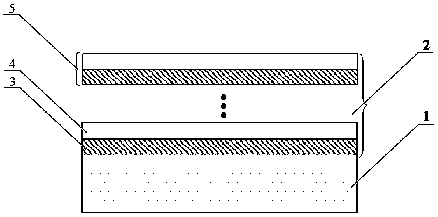
[0034] A bandgap-tunable photonic crystal back reflector, suitable for single-junction amorphous silicon thin-film solar cells, such as figure 1As shown, a substrate 1 is included, which is composed of a low-refractive-index silicon oxide film 3 and a high-refractive-index hydrogenated amorphous silicon film 4 periodically overlapped, the total number of periods is 5, and the thickness of the period is 200nm.

[0035] The silicon oxide film is prepared by RF-PECVD, the gas source is silane, hydrogen and carbon dioxide, the refractive index is 1.5, the thickness is 170nm, and the deposition parameters are as follows: power density 150mW / cm 2 , temperature 200°C, air pressure 200Pa, silane flow rate 30SCCM, hydrogen flow rate 60SCCM, carbon dioxide flow rate 20SCCM, deposition time 8min.

[0036] The hydrogenated amorphous silicon film is prepared by RF-PECVD, the gas source is silane and hydrogen, the refractive index is 4.5, the thickness is 30nm, and the deposition parameters...

Embodiment 2

[0039] A photonic crystal back reflector with adjustable bandgap, suitable for double-junction amorphous silicon / microcrystalline silicon stacked solar cells, such as figure 1 As shown, it includes a substrate 1, which is composed of a low-refractive-index silicon oxide film 3 and a high-refractive-index hydrogenated amorphous silicon film 4 periodically overlapped, the total number of periods is 5, and the thickness of the period is 250nm. The silicon oxide film is prepared by RF-PECVD, the gas source is silane, hydrogen and carbon dioxide, the refractive index is 1.5, the thickness is 200nm, and the deposition parameters are as follows: power density 150mW / cm 2 , temperature 200°C, air pressure 200Pa, silane flow rate 30SCCM, hydrogen flow rate 60SCCM, carbon dioxide flow rate 20SCCM, deposition time: 11min.

[0040] The hydrogenated amorphous silicon film is prepared by RF-PECVD, the gas source is silane and hydrogen, the refractive index is 4.5, and the thickness is 50nm. ...

Embodiment 3

[0043] A bandgap adjustable photonic crystal back reflector, suitable for triple-junction amorphous silicon / amorphous silicon germanium / microcrystalline silicon stacked solar cells, such as figure 1 As shown, it includes a substrate 1, which is composed of a low-refractive index silicon oxide film 3 and a high-refractive index hydrogenated amorphous silicon film 4 periodically overlapped, the total number of periods is 5, and the thickness of the period is 280nm. The silicon oxide film is prepared by RF-PECVD, the gas source is silane, hydrogen and carbon dioxide, the refractive index is 1.5, the thickness is 200nm, and the deposition parameters are as follows: power density 150mW / cm 2 , temperature 200°C, air pressure 200Pa, silane flow rate 30SCCM, hydrogen flow rate 60SCCM, carbon dioxide flow rate 20SCCM, deposition time 11min.

[0044] The hydrogenated amorphous silicon film is prepared by RF-PECVD, the gas source is silane and hydrogen, the refractive index is 4.5, and t...


PUM


Abstract

The invention discloses a photonic crystal back reflector provided with an adjustable forbidden band and applied to a silicon-based thin-film solar cell. The photonic crystal back reflector is composed of low-refraction-index media and high-refraction-index media which are overlapped in a periodic mode. Through adjustment of the thickness of a period, an average reflectivity of 96% can be obtained in a wave band of 500-750mm, an average reflectivity of 99% can be obtained in a wave band of 650-1100nm, and an average reflectivity of 99% can be obtained in a wave band of 700-1200nm. The photonic crystal back reflector is suitable for serving as a back reflector of a unijunction amorphous silicon thin film solar cell, a back reflector of a double-junction amorphous silicon/microcrystalline silicon laminated solar cell and a back reflector of a triple-junction amorphous silicon/amorphous silicon germanium/ amorphous silicon laminated solar cell. The photonic crystal back reflector provided with the adjustable forbidden band and applied to the silicon-based thin-film solar cell has the advantages that due to the fact that a photonic crystal is used as the back reflector of the silicon-based thin-film solar cell, the problems that an Ag back reflector is high in cost and other metal back reflectors are low in reflectivity are solved, high efficiency and decrease of the cost of raw materials are guaranteed, improvement of the open-circuit voltage of the cell is facilitated, the stability of the cell is improved, the photonic crystal back reflector is compatible with the cell technology, reduction of equipment investment and the plant area is facilitated, and productivity is improved.

Description

technical field [0001] The invention relates to the technical field of silicon-based thin-film solar cells, in particular to a bandgap-adjustable photonic crystal back reflector for silicon-based thin-film solar cells. Background technique [0002] Solar energy is an inexhaustible renewable energy source, which is of great significance to environmental protection. The effective use of solar energy has become the consensus of mankind. The use of solar energy, especially photovoltaic power generation technology, is the most promising renewable energy technology. Silicon-based thin-film solar cells have the advantages of low energy consumption, rich raw materials and no pollution, and easy large-scale production. They have been industrialized and their products are widely used in ground photovoltaic power stations, building integrated photovoltaics, and rooftop power stations. [0003] At present, silicon-based thin film solar cells that have been mass-produced mainly include ...

Claims


Application Information

Patent Timeline
Patent Type & Authority Applications(China)
IPC IPC(8): H01L31/20H01L31/0232H01L31/0224H01L31/0216H01L31/052
CPCY02E10/50Y02P70/50
Inventor 侯国付陈培专张建军倪牮张晓丹赵颖
Owner NANKAI UNIV
Why Eureka
Try Eureka