Preparation method of three-dimensional silicon nano structure for solar cell

A technology of solar cells and silicon nanometers, applied in nanotechnology, chemical instruments and methods, circuits, etc., can solve the problems of high reflectivity, achieve large specific surface area, controllable process, and enhance the effect of light trapping

Active Publication Date: 2013-10-02
SUZHOU INAINK ELECTRONICS MATERIALS CO LTD
View PDF3 Cites 22 Cited by
  • Summary
  • Abstract
  • Description
  • Claims
  • Application Information

AI Technical Summary

Problems solved by technology

However, the reflectivity of the pyramid-textured silicon surface is still high, especially the reflectivity of the short-wave band (visible light band) is more than 10%. Therefor

Method used


Image

  • Preparation method of three-dimensional silicon nano structure for solar cell
  • Preparation method of three-dimensional silicon nano structure for solar cell
  • Preparation method of three-dimensional silicon nano structure for solar cell

Examples


Example Embodiment

[0028] Embodiment one:

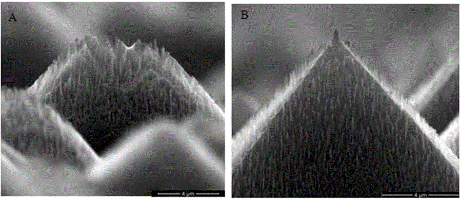
[0029] Put the cleaned silicon wafer into a mixed solution of 1.8% sodium hydroxide by mass and 10% ethanol by volume, and soak it at 80°C for 30 minutes to etch the "pyramid"-like suede structure; then remove Sodium hydroxide remaining on the surface of the silicon wafer, then remove the oxide layer on the surface of the silicon wafer, after further cleaning the silicon wafer, put it into 4.8M / L HF and 0.02M / L AgNO 3 In the mixed solution, silicon nanowires were etched at room temperature for 4 minutes, and then the removed silicon wafer was soaked in nitric acid for 1 hour, rinsed with deionized water after removal, and dried with a nitrogen gun to obtain a new three-dimensional Silicon nanostructure, its side SEM image is attached figure 2 shown.

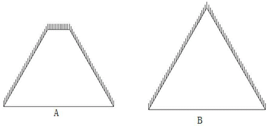
[0030] attached figure 1 It is a schematic diagram of the three-dimensional nanostructure prepared by the present invention, wherein A and B are respectively associated with the attached figure 2 co...

Example Embodiment

[0032] Embodiment two:

[0033] Put the cleaned silicon wafer into a mixed solution of 1.8% sodium hydroxide by mass and 10% ethanol by volume, and soak it at 80°C for 30 minutes to etch the "pyramid"-like suede structure; then remove Sodium hydroxide remaining on the surface of the silicon wafer, then remove the oxide layer on the surface of the silicon wafer, after further cleaning the silicon wafer, put it into 4.8M / L HF and 0.02M / L AgNO 3 In the mixed solution, silicon nanowires were etched at room temperature for 5 minutes, and then the removed silicon wafer was soaked in nitric acid for 1 hour, rinsed with deionized water after removal, and dried with a nitrogen gun to obtain a new three-dimensional Silicon nanostructures.

Example Embodiment

[0034] Embodiment three:

[0035] Put the cleaned silicon wafer into a mixed solution of 1.8% sodium hydroxide by mass and 10% ethanol by volume, and soak it at 80°C for 30 minutes to etch the "pyramid"-like suede structure; then remove Sodium hydroxide remaining on the surface of the silicon wafer, then remove the oxide layer on the surface of the silicon wafer, after further cleaning the silicon wafer, put it into 4.8M / L HF and 0.02M / L AgNO 3 In the mixed solution, silicon nanowires were etched at room temperature for 6 minutes, and then the removed silicon wafer was soaked in nitric acid for 1 hour, rinsed with deionized water after removal, and dried with a nitrogen gun to obtain a new three-dimensional Silicon nanostructures.


PUM


Abstract

The invention discloses a preparation method of a three-dimensional silicon nano structure for a solar cell. The preparation method aims at obtaining a silicon wafer with a large specific surface area, so that a light trapping effect of the silicon wafer on sunlight is improved. The preparation method comprises the steps that after the silicon wafer is cleaned, a pyramid-shaped suede structure is formed on the surface of the silicon wafer by utilizing the surface anisotropy corrosion of aqueous alkali on monocrystalline silicon, and a silicon nanowire is further etched on the pyramid suede structure by utilizing a metal ion-assisted chemical etching method, so that the novel silicon nanowire-pyramid three-dimensional silicon nano structure is formed. According to the preparation method, the novel three-dimensional silicon nano structure can provide the silicon wafer with the larger specific surface area, so that the light trapping effect of the surface of the silicon wafer on the sunlight is improved; the reflectivity of a short-wave band is less than 5%; the preparation method is low in cost, mild in condition and shorter in time; a technological process is controllable; and industrial operation is facilitated.

Description

technical field [0001] The invention belongs to the technical field of solar cell preparation, and in particular relates to a method for preparing a novel three-dimensional silicon nanostructure. Background technique [0002] With the rapid development of society, many available resources are facing the danger of being exhausted, and finding new energy to replace these resources that are about to be exhausted has become one of the urgent problems facing mankind. Because solar energy is a non-polluting, effective, renewable and clean energy, and its reserves are huge, inexhaustible, low cost of use, not limited by geographical conditions, etc., it is full of broad application prospects; and Solar power has cleanliness, safety, extensiveness and adequacy of resources that cannot be compared with thermal power, hydropower, and nuclear power. Therefore, solar energy is considered to be the energy source that has attracted the most attention and has the most development prospects...

Claims


Application Information

Patent Timeline
IPC IPC(8): H01L31/18C30B33/10H01L31/0236B82Y40/00
CPCY02E10/50Y02P70/50
Inventor 孙宝全张云芳
Owner SUZHOU INAINK ELECTRONICS MATERIALS CO LTD
Why Eureka
Try Eureka